Insulation sheet, multi-layer wiring substrate and production processes thereof

a technology of multi-layer wiring and substrate, applied in the direction of printed element electric connection formation, association of printed circuit non-printed electric components, conductive pattern formation, etc., can solve the problems of high cost, and high cost of chemical plating treatmen

Inactive Publication Date: 2005-02-15
PANASONIC CORP
View PDF10 Cites 60 Cited by
  • Summary
  • Abstract
  • Description
  • Claims
  • Application Information

AI Technical Summary

Problems solved by technology

This process for forming the via holes, however, has problems in terms of productivity and cost; that is, chemicals for use in a chemical plating treatment are expensive, and this treatment requires much time.
In a case where a wiring substrate having a plurality of wiring layers is produced, it is difficult to form via hole conductors capable of performing electrical connection at any optionally predetermined positions between the wiring layers, and therefore, it is difficult to form a wiring layer having a high density wiring pattern thereon.
However, when heated, the thermosetting resins have a lower viscosity with rise in temperature, or are melted and converted from solids into fluids having a very high viscosity (in this state, they are tacky).
With further rise in temperature, viscosity of the thermosetting resins further decreases, so that, the resins are not able to, or almost unable to, maintain their forms which the resins have at a room temperature, even without any external force applied thereto(namely, naturally); that is, the resins become flowable.
As a result, application of a sufficient pressure is impossible because shapes of the via holes tend to deform.
Under an insufficient pressure, the conductive paste in the via holes cannot be sufficiently compressed up to a high density, so that there arises a problem in that highly reliable electrical connection becomes impossible, and a problem that positions of the via holes are dislocated from original positions at which the via holes have been formed through the insulation sheet, with a result of poor positional accuracy of the via holes.
There is a further problem in that, when the insulation sheet melts and becomes flowable, the conductive paste overflows from the via holes and adheres to a surface of the insulation sheet and an unintended region other than a predetermined region between a wiring layer and a via hole conductor, with a result that a short circuit is formed by this attaching paste between adjacent wiring conductors.
The foregoing problem in association with flowing of the insulation sheet itself, therefore, becomes more serious.
Therefore, it is very difficult to achieve at the same time both objects; that is, to achieve high density mounting of circuit components by embedding the circuit components in the insulation sheet, and to accomplish high density wiring by a shortest electrical connection through inner via holes filled with conductive paste.

Method used


Image

  • Insulation sheet, multi-layer wiring substrate and production processes thereof
  • Insulation sheet, multi-layer wiring substrate and production processes thereof
  • Insulation sheet, multi-layer wiring substrate and production processes thereof

Examples


embodiment 1

Concrete Embodiment 1 for Carrying out the Invention)

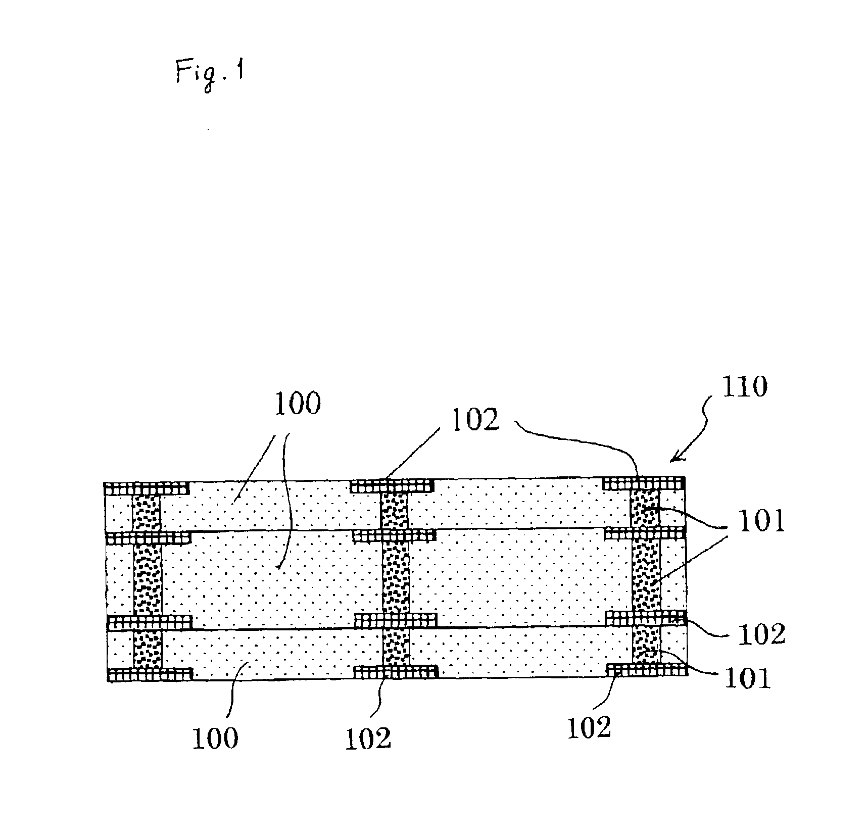
FIG. 1 schematically shows a sectional view of a multi-layer wiring substrate (110) (four layers in the shown embodiment) according to one embodiment of the present invention. The wiring substrate (110) comprises insulating layers (100) formed of insulation sheets, via hole conductors (101) formed by filling via holes with conductive paste which starts curing at a temperature lower than a melting-starting temperature of the insulation sheets, and wiring layers (102) which provide metal wirings.

In the present invention, the via hole conductors (101) are formed of the conductive paste which starts curing at a temperature lower than the melting-starting temperature of the insulation sheets. By doing so, the via hole conductors can have an effect to maintain their shapes against melting and flowing of the insulation sheets. As a result, the via hole conductors comprising the conductive paste can be compressed, and conductive powder in...

embodiment 2

(Concrete Embodiment 2 for Carrying Out the Invention)

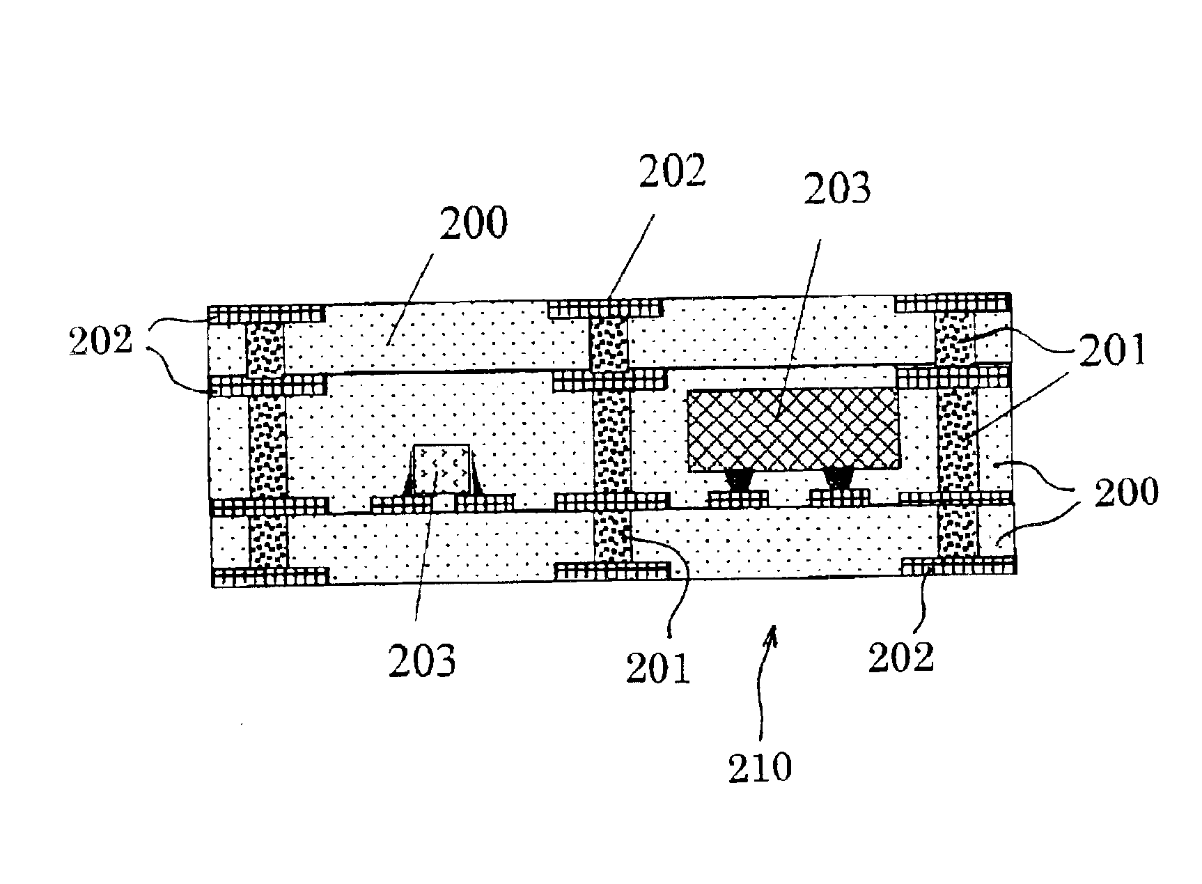
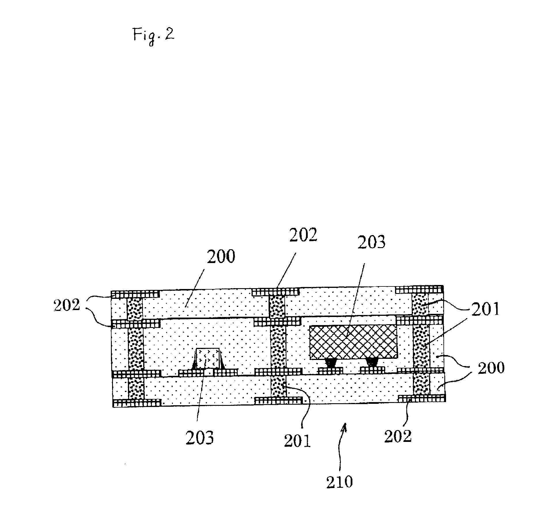
FIG. 2 schematically shows a sectional view of a circuit component-embedded multi-layer wiring substrate (210) (four layers in the shown embodiment) according to one embodiment of the present invention. The wiring substrate (210) comprises insulating layers (200) formed of insulation sheets, via hole conductors (201) formed by filling via holes with conductive paste which starts curing at a temperature lower than a melting-starting temperature of the insulation sheets, and wiring layers (202) which provide metal wirings, with one of the insulating layers (200) having embedded circuit components (203) electrically connected to the wiring layers.

Also, the multi-layer wiring substrate shown in FIG. 2 provides effects which are equivalent to those previously described with reference to FIG. 1. Regarding the insulating layer having the circuit components embedded therein, both of high density mounting of the circuit components by embe...

embodiment 3

(Concrete Embodiment 3 for Carrying Out the Invention)

A concrete embodiment of a process for producing the multi-layer wiring substrate of the present invention is described with reference to schematic sectional views shown in FIGS. 3(a) to 3(i).

An uncured insulation sheet (300) containing an inorganic filler and a thermosetting resin, which forms an insulating layer, is prepared (see FIG. 3(a)), and via holes (301) are formed through the insulation sheet (300) (see FIG. 3(b)). The via holes (301) formed through the insulation sheet (300) are filled with conductive paste, which starts curing at a temperature lower than a melting-starting temperature of the insulation sheet (300), so as to form via hole conductors (302). Thus, an insulation sheet (310) of the present invention is obtained (see FIG. 3(c)). In parallel to the steps shown in FIGS. 3(a) to 3(c), a transferable wiring pattern-including member (315) is prepared (see FIG. 3(d)). The transferable wiring pattern-including mem...


PUM

PropertyMeasurementUnit
temperatureaaaaaaaaaa
weight ratioaaaaaaaaaa

Abstract

An insulation sheet for use in producing a wiring substrate comprises, as via bole conductors, conductive paste filled in via holes formed through the insulation sheet, and a curing-starting temperature of the conductive paste is lower than a melting-starting temperature of the insulation sheet. A wiring substrate is produced by laminating such insulation sheets, that have conductive paste in via holes, and subjecting this laminate to thermo-compression bonding, wherein deformation of via holes and dislocation of the via holes, because of a molten insulation sheet, does not occur.

Description

CROSS-REFERENCE OF RELATED APPLICATIONThe present application claims priority under the provision of Article 119 of U.S. Patent Law, on basis of Japanese Patent Application No. 2001-296819, entitled “Multi-Layer Wiring Substrate and Circuit Component Including Multi-Layer Wiring Substrate, and Production Processes Thereof”, filed on Sep. 27, 2001, and the contents of this application are incorporated into the present specification by this citation.FIELD OF THE INVENTIONThe present invention relates to a both-sided wiring substrate (or board) in which electric connection is performed through via hole conductors provided by forming via holes through an insulating layer containing at least an organic resin, and filling the via holes with electrically conductive paste. The present invention also relates to a circuit component-including both-sided wiring substrate, a multi-layer wiring substrate and a circuit component-including multi-layer wiring substrate, and production methods of the...

Claims


Application Information

Patent Timeline
Patent Type & Authority Patents(United States)
IPC IPC(8): H05K3/40H05K3/46H05K1/18
CPCH05K3/4069H05K3/4617H01L2224/16Y10T29/49165H01L2924/01078H01L2924/01079H05K1/185H05K3/4626H05K3/4652H05K3/4655H05K2201/0209H05K2201/10378H01L2924/01019Y10T29/49155H01L2924/01046Y10T428/249996H05K3/46
Inventor KOMATSU, SHINGONAKATANI, SEIICHISUGAYA, YASUHIROASAHI, TOSHIYUKIYAMAMOTO, YOSHIYUKI
Owner PANASONIC CORP
Why Eureka
Try Eureka