

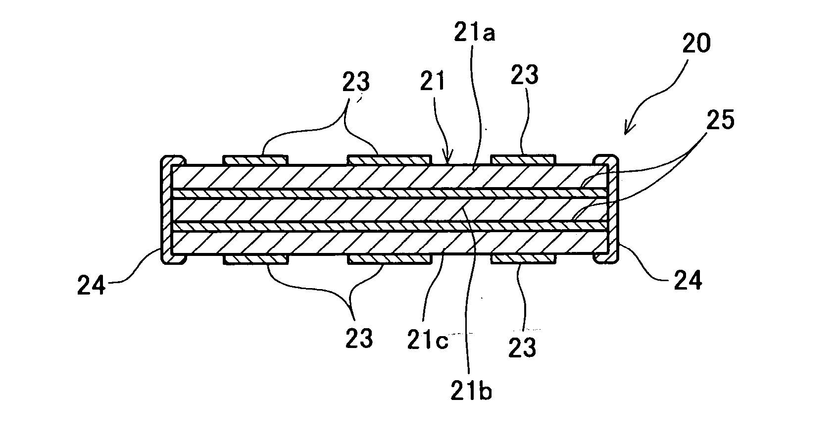
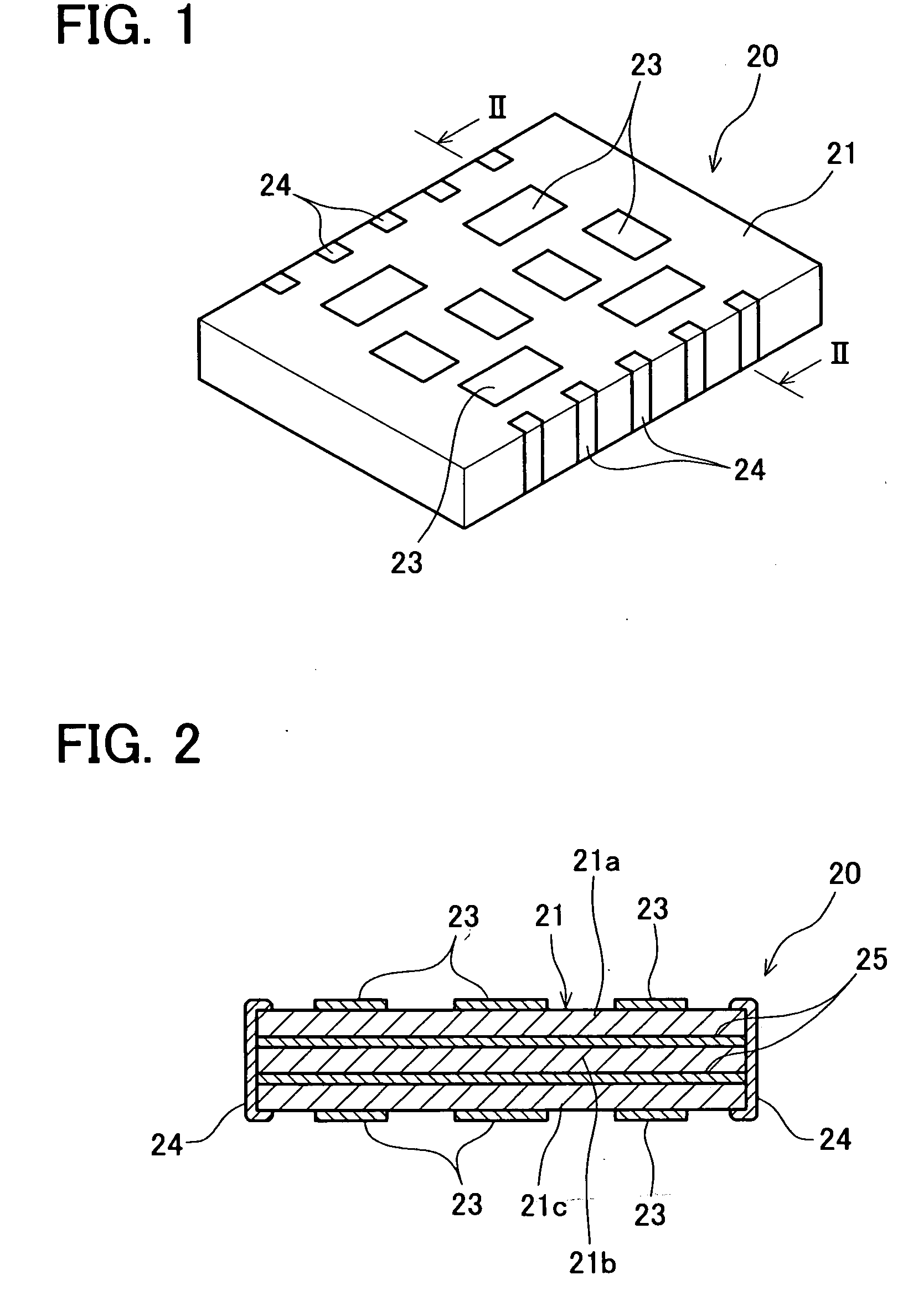
Ceramic electronic component and production method therefor
a technology of ceramic electronic components and production methods, applied in the direction of fixed capacitors, heat inorganic powder coatings, non-conductive materials with dispersed conductive materials, etc., can solve the problem of insufficient consideration of ag paste as one base, and achieve the effect of improving electrical characteristics and/or mechanical characteristics, and improving quality
- Summary
- Abstract
- Description
- Claims
- Application Information
AI Technical Summary
Benefits of technology
Problems solved by technology
Method used
Image

Examples
production example 2
Preparation of Ag Paste for Surface Film Conductor Formation
[0080] Twelve types of Ag paste for surface film conductor formation having compositions shown as No. 11 to No. 22 in Tables 2 to 4 were prepared.
[0081] The same type of Ag powder and metal alkoxide as used in Production Example 1 were used. That is, Ag powders having an average particle size of 0.3 to 0.5% m for Nos. 16, 17, 20 to 22; an average particle size of 0.6 to 0.8 .mu.m for Nos. 11, 14, 15, 18 and 19; an average particle size of 0.8 to 1.0 .mu.m for No. 12; an average particle size of 1.5 to 2.0 .mu.m for No. 13 were used. Acetoalkoxy aluminum diisopropylate was used for Nos. 11, 14 to 19, 21 and 22, and zirconium butoxide was used for Nos. 12, 13 and 20.
[0082] Thus, coating solutions having a metal alkoxide concentration of 5 to 100 g / l were prepared, and the same treatments as in Production Example 1 were performed. Then, coated Ag powders in which the surface was coated substantially uniformly with aluminum alk...
PUM
| Property | Measurement | Unit |
|---|---|---|
| Temperature | aaaaa | aaaaa |
| Temperature | aaaaa | aaaaa |
| Fraction | aaaaa | aaaaa |
Abstract
Description
Claims
Application Information