Time Resolved Photoluminescence Imaging Systems And Methods For Photovoltaic Cell Inspection

A photoluminescence, photovoltaic cell technology, applied in TV, electrical components, image communication and other directions, can solve problems such as disadvantages

Inactive Publication Date: 2013-01-02
INTEVAC
View PDF6 Cites 15 Cited by
  • Summary
  • Abstract
  • Description
  • Claims
  • Application Information

AI Technical Summary

Problems solved by technology

[0007] Existing steady-state photoluminescent signaling techniques are disadvantageous because they require calibration to convert the signal into an effective lifetime

Method used


Image

  • Time Resolved Photoluminescence Imaging Systems And Methods For Photovoltaic Cell Inspection
  • Time Resolved Photoluminescence Imaging Systems And Methods For Photovoltaic Cell Inspection
  • Time Resolved Photoluminescence Imaging Systems And Methods For Photovoltaic Cell Inspection

Examples


Embodiment Construction

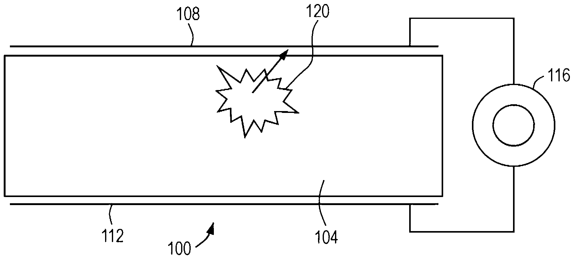
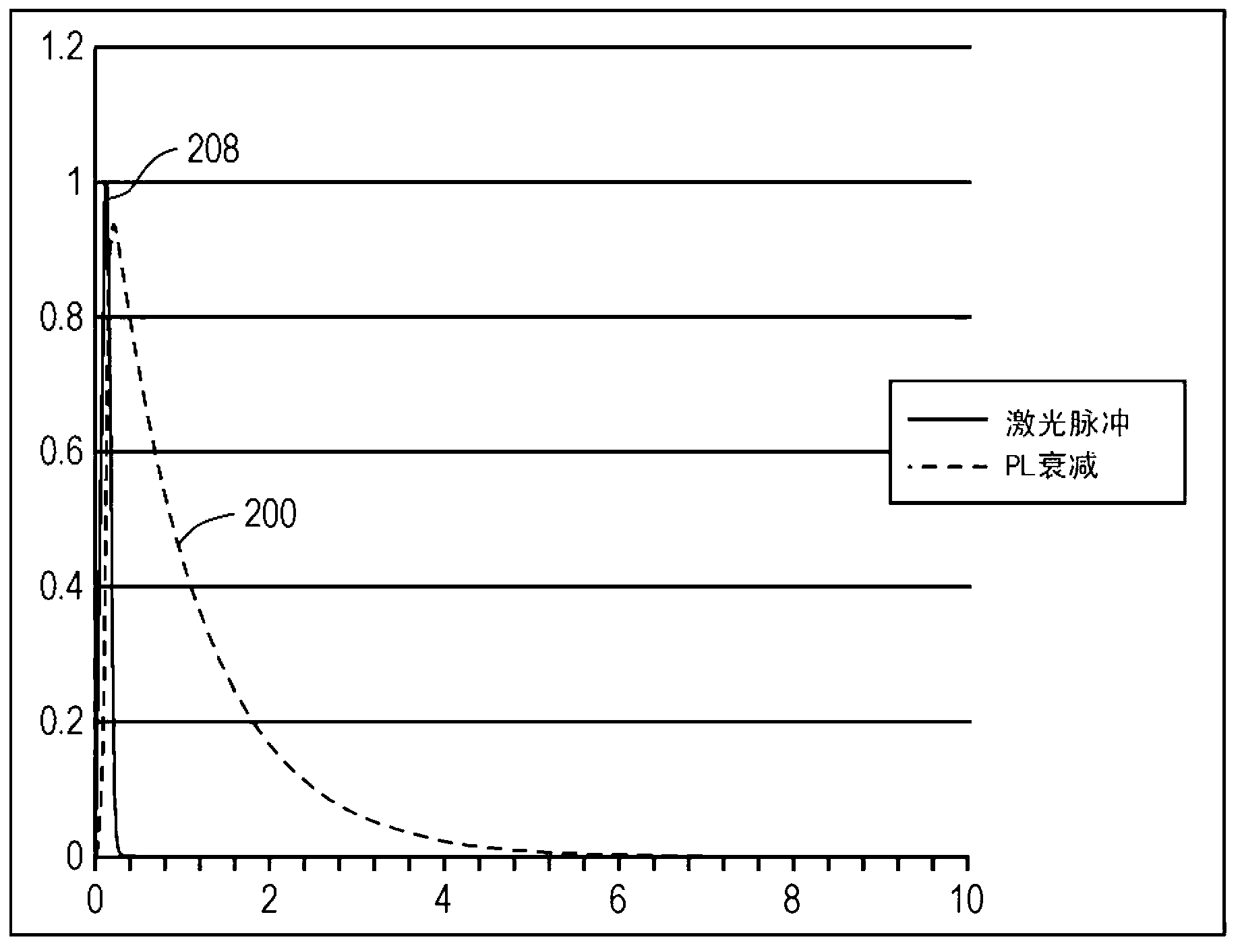
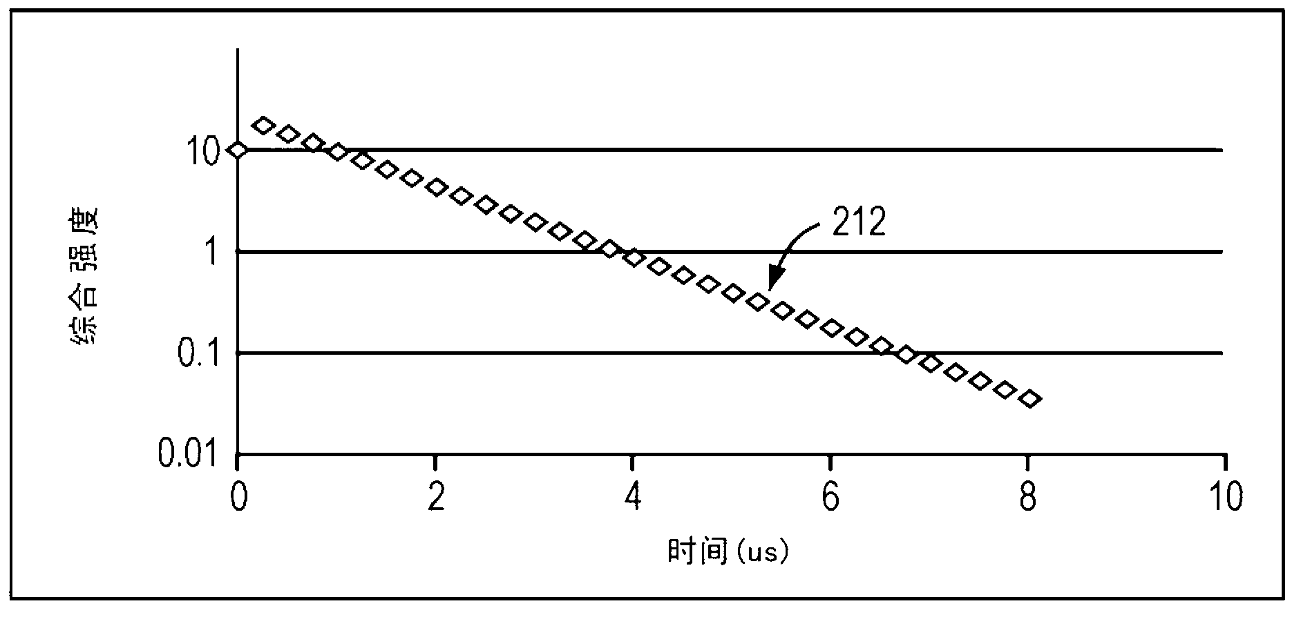
[0039] A time-resolved photoluminescence technique for imaging and inspecting photovoltaic cells is disclosed. The photoluminescence intensity is proportional to the carrier lifetime: -I PL =cΔn=cT, where n is the carrier charge density, c is a constant, and T is the lifetime. A pulsed light source flashes the wafer, generating excess carriers in the silicon, causing photoluminescence. The carrier recombination rate was monitored by imaging the photoluminescence decay as a function of time using a photodetector with a fast response. Photoluminescence decay curves were generated and effective lifetimes were extracted from the curves. Therefore, the effective lifetime was measured directly.

[0040] will now refer to figure 1 Embodiments of the present invention are described in detail. figure 1An exemplary photovoltaic cell 100 is shown. A photovoltaic cell typically includes a semiconductor wafer 104 that converts energy from sunlight into electricity. Semiconductor waf...


PUM


Abstract

A time-resolved photoluminescence technique is disclosed to image photovoltaic cells and wafers. The effective lifetime is measured directly using a photodetector that has a fast response. A pulsed light source flashes the wafer, generating excess carriers in the silicon. The rate of carrier recombination is monitored by imaging the photoluminescence decay over time. An effective lifetime can be extracted from the photoluminescence decay curve, which can be used to determine the quality of the photovoltaic cells and wafers.

Description

[0001] Cross references to related patent applications [0002] This application claims priority to Provisional Application No. 61 / 318738, filed March 29, 2010, the disclosure of which is hereby incorporated by reference in its entirety. technical field [0003] The subject invention relates to time resolved photoluminescence imaging systems and methods of photovoltaic cell inspection. Background technique [0004] Photoluminescence is the re-emission of light following absorption of higher energy (shorter wavelength) light. Visible light from solar lamps, lasers or LEDs excites electrons in photovoltaic wafer materials such as silicon. Most of the photogenerated electrons give their energy in the form of heat, but a small fraction recombine with holes in the silicon, emitting photons (radiative recombination). More defects in silicon result in more energy being lost as heat and fewer photons are emitted, while fewer defects in silicon result in more radiative recombinatio...

Claims


Application Information

Patent Timeline
Patent Type & Authority Applications(China)
IPC IPC(8): G01J3/40
CPCH04N7/183G01N21/6489G01N21/6408G01N21/9501G01N2021/646
Inventor B·特鲁
Owner INTEVAC
Why Eureka
Try Eureka