
Bootstrap type charging circuit applied to high-voltage DC-DC (Direct Current-Direct Current) convertor

A DC-DC and charging circuit technology, applied in the direction of conversion equipment without intermediate conversion to AC, can solve the problems of inability to fully drive the main switch tube, slow charging speed of C0, and drop in bootstrap voltage, so as to improve the charging driving ability , Accelerate the charging speed and increase the working voltage range

Active Publication Date: 2013-01-09
深圳德信微电子有限公司
View PDF5 Cites 11 Cited by
  • Summary
  • Abstract
  • Description
  • Claims
  • Application Information

AI Technical Summary

Problems solved by technology

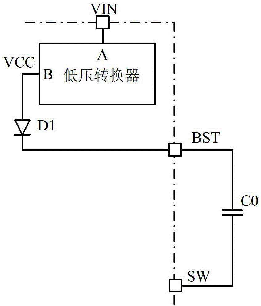
At this time, the traditional bootstrap charging circuit will cause the charging speed of C0 to be too slow to make up for the loss when the bootstrap voltage drives the upper transistor to be turned on in the next cycle, causing the bootstrap voltage to drop and unable to fully drive the main switch.

Method used


Image

  • Bootstrap type charging circuit applied to high-voltage DC-DC (Direct Current-Direct Current) convertor
  • Bootstrap type charging circuit applied to high-voltage DC-DC (Direct Current-Direct Current) convertor
  • Bootstrap type charging circuit applied to high-voltage DC-DC (Direct Current-Direct Current) convertor

Examples


Embodiment 1

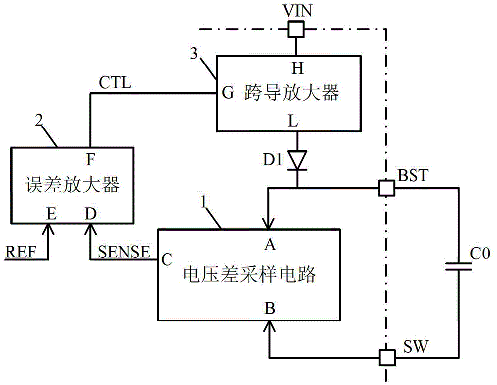
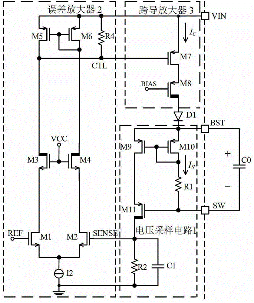
[0051] refer to image 3 , the voltage difference sampling circuit 1, error amplifier 2 and transconductance amplifier 3 that the bootstrap circuit of the present invention comprises, its specific circuit structure is as follows:

[0052] The voltage difference sampling circuit 1 of the present invention includes a high-voltage PMOS transistor M11 with a withstand voltage greater than 12V between the source and the drain, low-voltage PMOS transistors M9 and M10, resistors R1 and R2, and a capacitor C1;

[0053] The source of the low-voltage PMOS transistor M9 and M10 is connected, and as the input terminal A of the voltage difference sampling circuit 1, it is connected to the output pin BST of the DC-DC converter; its gate is connected to form an active current mirror structure ; The drain of the low-voltage PMOS transistor M10 is connected to the output pin BST of the DC-DC converter through the series resistor R1, and is used to sample the voltage difference V between the ou...

Embodiment 2

[0065] refer to Figure 4 , the voltage difference sampling circuit 1, error amplifier 2 and transconductance amplifier 3 that the bootstrap circuit of the present invention comprises, its specific circuit structure is as follows:

[0066] The voltage difference sampling circuit 1 and the transconductance amplifier 3 of the present invention are the same as those of the first embodiment.

[0067] The error amplifier 2 of the present invention includes high-voltage NMOS transistors M3, M4, M14, and M15 with withstand voltages greater than 12V between source and drain, low-voltage NMOS transistors M1, M2, M16, and M17, and low-voltage PMOS transistors M5, M6, and M12. , M13, resistor R4 and current source I2;

[0068] The low-voltage NMOS transistor M1 is connected to the source of M2 to form a differential pair, which is connected to the current source I2; its grid is respectively used as the input terminal E and the input terminal D of the error amplifier 2, and the input ter...

Embodiment 3

[0075] refer to Figure 5 , the voltage difference sampling circuit 1, error amplifier 2 and transconductance amplifier 3 that the bootstrap circuit of the present invention comprises, its specific circuit structure is as follows:

[0076] The voltage difference sampling circuit 1 and the transconductance amplifier 3 of the present invention are the same as those of the first embodiment.

[0077] The error amplifier 2 of the present invention includes high-voltage NMOS transistors M3, M4, M14, and M15 with withstand voltages greater than 12V between source and drain, low-voltage NMOS transistors M1, M2, M16, and M17, and low-voltage PMOS transistors M5, M6, and M12. , M13, resistor R4 and current source I2;

[0078] The low-voltage NMOS transistor M1 is connected to the source of M2 to form a differential pair, which is connected to the current source I2; its grid is respectively used as the input terminal E and the input terminal D of the error amplifier 2, and the input ter...


PUM


Abstract

The invention discloses a bootstrap type charging circuit applied to a high-voltage DC-DC (Direct Current-Direct Current) convertor. The problems that the conventional internal power supply driving capacity is limited, and bootstrap voltage relies on SW voltage of an output pin of the DC-DC converter can be mainly solved. The bootstrap type charging circuit comprises a voltage difference sampling circuit (1), an error amplifier (2) and a trans-conductance amplifier (3); the voltage difference sampling circuit converts the difference value of the output pin BST and the output pin SW of the DC-DC converter into a voltage difference signal SENSE; the voltage difference signal and reference voltage REF (Reference) inside the DC-DC converter is subjected to differential amplification through an error amplifier, so as to output a difference signal CTL; the difference signals are converted into a current signal through the trans-conductance amplifier, and is connected with a voltage difference sampling circuit through a diode, so as to form a negative feedback control loop; and the trans-conductance amplifier uses high-voltage power supply VIN through the DC-DC converter, so as to ensure that the charging current is directly supplied by a chip power source. With the adoption of the bootstrap type charging circuit provided by the invention, the driving capacity of a main switch tube can be effectively improved; the stability of the bootstrap voltage can be ensured; the bootstrap type charging circuit does not rely on the SW voltage of the output end, and can be used for the large-load DC-DC converter.

Description

technical field [0001] The invention belongs to the technical field of electronic circuits, and relates to an analog integrated circuit, in particular to a bootstrap charging circuit applied to a high-voltage DC-DC converter. Background technique [0002] In the field of power management, the main switching tubes of high-voltage DC-DC converters all use NMOS type, because NMOS has smaller on-resistance than PMOS in the same area, thus saving more area. The source of the NMOS is the output pin SW of the DC-DC converter, and the drain is connected to the input pin VIN of the DC-DC converter. Therefore, the main switch needs a gate driving voltage higher than the voltage of the output pin SW to drive the main switch to conduct. But when the main switch is turned on, the voltage of the output pin SW is almost equal to the voltage of the input pin VIN, and there is no voltage higher than the voltage of the input pin VIN in the circuit to drive the gate of the main switch. There...

Claims


Application Information

Patent Timeline
Patent Type & Authority Applications(China)
IPC IPC(8): H02M3/07
Inventor 来新泉刘雨鑫叶强邵丽丽卓越
Owner 深圳德信微电子有限公司
Learn More