Novel laminated diode manufacturing process and chip sieve tray thereof

A technology of manufacturing process and chip sieve tray, which is applied in semiconductor/solid-state device manufacturing, electrical components, circuits, etc., can solve the problems of chip surface damage, improvement, and restriction of electrical yield, so as to improve efficiency and accuracy, improve The effect of work efficiency

Active Publication Date: 2013-01-16
RUGAO DACHANG ELECTRONICS
View PDF8 Cites 9 Cited by
  • Summary
  • Abstract
  • Description
  • Claims
  • Application Information

AI Technical Summary

Problems solved by technology

For the products produced by the above process, when the polarity is manually identified, the chip with the opposite polarity will be adjusted, and the tweezers used in the adjustment process will cause damage to the chip table, which restricts the electrical yield of this product. Improvement (the current industry electrical yield rate is 85%)

Method used


Image

  • Novel laminated diode manufacturing process and chip sieve tray thereof
  • Novel laminated diode manufacturing process and chip sieve tray thereof
  • Novel laminated diode manufacturing process and chip sieve tray thereof

Examples


Embodiment Construction

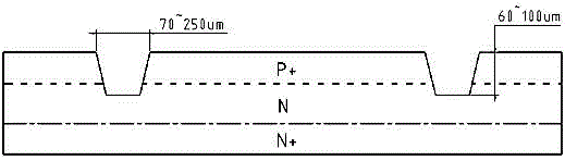
[0015] Such as figure 1 As shown, a wide groove is opened on the P side (or N side) of the silicon wafer, the groove width is 70~250um, and the groove depth is 60~100um (see figure 1 Medium size), adjust the groove width and groove depth in the above range according to the specific product requirements.

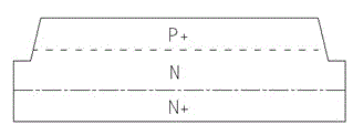
[0016] Such as figure 2 As shown, scribing is performed with the center of the bottom of the wide groove as the boundary, and the width of the scribing lane is about 50um, thereby forming a chip with a small face and a large face.

[0017] In the process of grooving and scribing on the P side (or N side) of the silicon wafer, by adjusting the chip size, the size of the small side is properly compensated, so as to meet the electrical parameter requirements of the product. The specific method is the same as the compensation principle of the size and surface area of ​​the GPP chip known in the industry, and will not be repeated here.

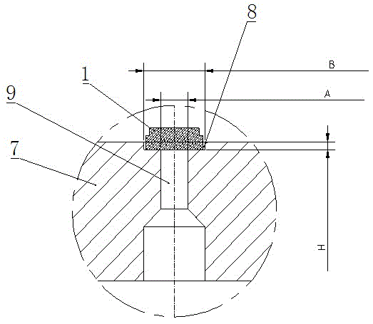
[0018] Such as image 3 As shown, lead...


PUM


Abstract

The invention relates to a novel laminated diode manufacturing process and a chip sieve tray thereof. The novel laminated diode manufacturing process is characterized by comprising the following steps of forming a wide groove in the P surface or the N surface of a silicon wafer, wherein the groove is 70 to 250 mum in width and 60 to 100 mum in depth; scribing in the way that the center of the bottom of the wide groove serves as a boundary; after filling a lead and sieving a chip, welding and fixing the chip and the lead by using a welding material, and when the chip is sieved, matching a small surface formed by forming the wide groove with a profile hole of the chip sieve tray to identify the polarity of the P surface or the N surface; and sequentially performing acid washing, strip combing, sizing, glue curing, mould pressing, post curing, electroplating, testing, character printing, packaging and goods delivery. Due to the steps of forming the wide groove in the P surface or the N surface of the silicon wafer, scribing in the way that the center of the bottom of the wide groove serves as the boundary, matching the small surface formed by forming the wide groove with the profile hole of the chip sieve tray to automatically identify and adjust the polarity of the P surface or the N surface, manual identification is not required, the efficiency and the accuracy are effectively improved, and the damage to the chip caused by manual adjustment with a nipper is avoided.

Description

technical field [0001] The invention relates to a novel laminated diode manufacturing process, in particular to a chip sieve plate for realizing the novel laminated diode manufacturing process. Background technique [0002] At present, the laminated diode series products on the market are all produced by the traditional coloring lamination process (the purpose of coloring is to distinguish the PN polarity of the diode). The disadvantages of this process are low chip loading efficiency and high labor costs. The specific process is as follows: silicon wafer P-side coloring→scribing→lead wire filling→sieving chips (manual identification of polarity)→soldering→acid cleaning→combing strips→gluing→glue curing→molding→post-curing→electroplating→testing , Printing→packaging→shipping. For the products produced by the above process, when the polarity is manually identified, the chip with the opposite polarity will be adjusted, and the tweezers used in the adjustment process will cau...

Claims


Application Information

Patent Timeline
Patent Type & Authority Applications(China)
IPC IPC(8): H01L21/329H01L21/67
Inventor 赵宇
Owner RUGAO DACHANG ELECTRONICS
Why Eureka
Try Eureka