Method for aligning exposure patterns on two sides of PCB (printed circuit board)

A PCB board and exposure pattern technology, which is applied in the field of realizing the alignment of exposure patterns on both sides of the PCB board, can solve the problems that the position change of the circuit board cannot be measured, and the position of the exposure pattern has no way to correspond one-to-one, so as to improve the accuracy and eliminate the alignment The influence of precision and the effect of simplifying the process flow

Inactive Publication Date: 2013-01-23
TIANJIN ADVANTOOLS
View PDF6 Cites 31 Cited by
  • Summary
  • Abstract
  • Description
  • Claims
  • Application Information

AI Technical Summary

Problems solved by technology

If the system cannot measure the position changes of the two circuit board placements before and after when exposing the reverse side, then there is no way to correspond the positions of the exposure patterns on the front and back sides of the same circuit board

Method used


Image

  • Method for aligning exposure patterns on two sides of PCB (printed circuit board)
  • Method for aligning exposure patterns on two sides of PCB (printed circuit board)
  • Method for aligning exposure patterns on two sides of PCB (printed circuit board)

Examples


Embodiment Construction

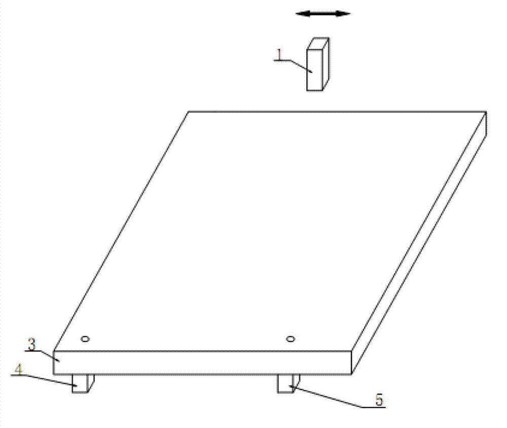
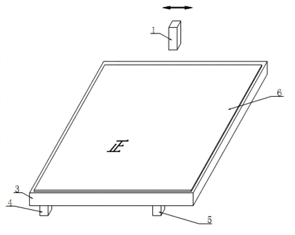
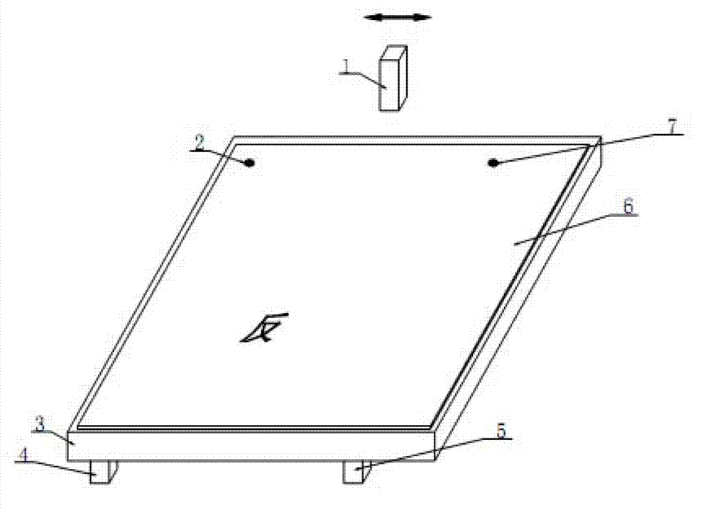
[0020] Such as figure 2 As shown, in the laser imaging system, the alignment method for realizing the alignment of exposure patterns on both sides of the circuit board is characterized in that a PCB board 6 is placed on the workpiece table 3, a CCD camera 1 is arranged above the PCB board 6, and a CCD camera 1 is arranged below the workpiece table 3. There are marking device 1 4 and marking device 2 5, and the workpiece table 3 is provided with two through holes for marking device 1 4 and marking device 2 5 to generate specific alignment marks on the PCB board 6;

[0021] Specifically include the following steps:

[0022] 1) if figure 1 As shown, use the CCD camera 1 to calibrate the position coordinates of the marking device 1 4 and the marking device 2 5 fixed below the workpiece table 3;

[0023] 2) if figure 2 As shown, the PCB board 6 is placed on the workpiece table 3, while the front side of the PCB board is exposed, the marking device 1 4 generates alignment marks...


PUM


Abstract

The invention discloses an alignment method for aligning exposure patterns on two sides of a PCB (printed circuit board). The PCB is placed on a work piece table, a CCD (charge coupled device) camera is arranged on the PCB, and a marking device is arranged below the PCB; and when the front side of the PCB is exposed, the marking device can generate alignment marks on the reverse side of the PCB, and after the PCB is turned over, the CCD camera can capture the alignment marks on the reverse side for alignment, so that the exposure patterns on the two sides of the PCB can be aligned. According to the invention, the alignment of the exposure patterns on the two sides of the PCB can be implemented, the procedure is simple and the alignment accuracy is high.

Description

technical field [0001] The invention relates to the technical field of printed circuit board equipment, in particular to a method for realizing alignment of exposure patterns on both sides of a PCB board. Background technique [0002] The exposure alignment method of the laser direct writing exposure machine is to extract and calculate the center coordinates of the alignment holes or feature graphics on the PCB and the center coordinates of the alignment points on the CAM image, so that the CAM image can be rotated and translated to realize the CAM graphics The principle of matching with the PCB board. However, in some circuit board production processes, there is no alignment hole or characteristic pattern on the inner layer board. The traditional exposure machine uses side-by-side double-sided simultaneous exposure, and the alignment is performed on both sides when setting up the negative. The laser direct writing exposure machine does not expose both sides at the same tim...

Claims


Application Information

Patent Timeline
Patent Type & Authority Applications(China)
IPC IPC(8): G03F7/20G03F9/00
Inventor 吴俊
Owner TIANJIN ADVANTOOLS
Why Eureka
Try Eureka