Method for locating Mark points on PCB (printed circuit board) by utilizing outline gravity center method

A technology of PCB board and center of gravity method, which is used in instruments, character and pattern recognition, computer parts and other directions, and can solve problems such as inability to handle sub-pixel levels and false alarms.

Active Publication Date: 2013-02-13
廖怀宝
View PDF1 Cites 26 Cited by
  • Summary
  • Abstract
  • Description
  • Claims
  • Application Information

AI Technical Summary

Problems solved by technology

But this method can only deal with the pixel level, not the sub-pixel level
Moreover, this method is affected by the external light. When the external light source changes greatly, this method will cause false positives.

Method used


Image

  • Method for locating Mark points on PCB (printed circuit board) by utilizing outline gravity center method
  • Method for locating Mark points on PCB (printed circuit board) by utilizing outline gravity center method

Examples


Embodiment Construction

[0027] The solution of the present invention will be described in detail below in conjunction with the accompanying drawings.

[0028] The present invention adopts the contour center of gravity method to locate the PCB board. The so-called contour center of gravity method is to extract the contour center of gravity of the Mark point of the board to be detected first, and use the reference Mark point (the reference Mark point refers to the Mark point extracted by us when programming) and the detection Mark point. The offset between the centers of gravity is used for PCB board compensation. The specific operation steps are as follows:

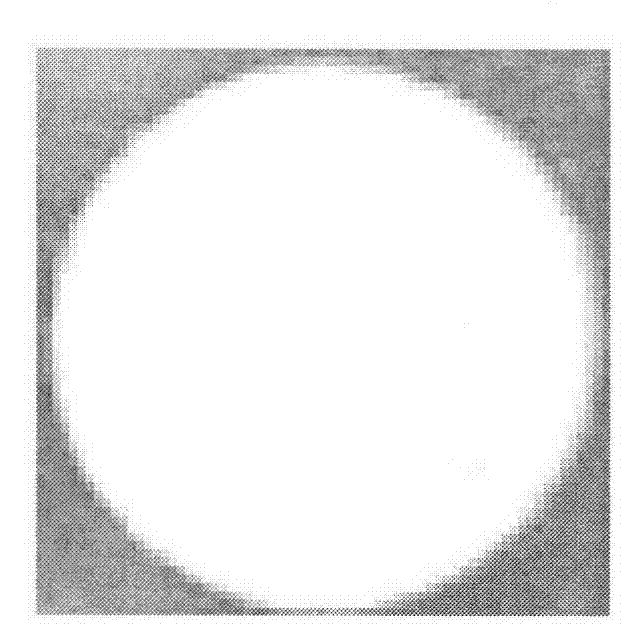
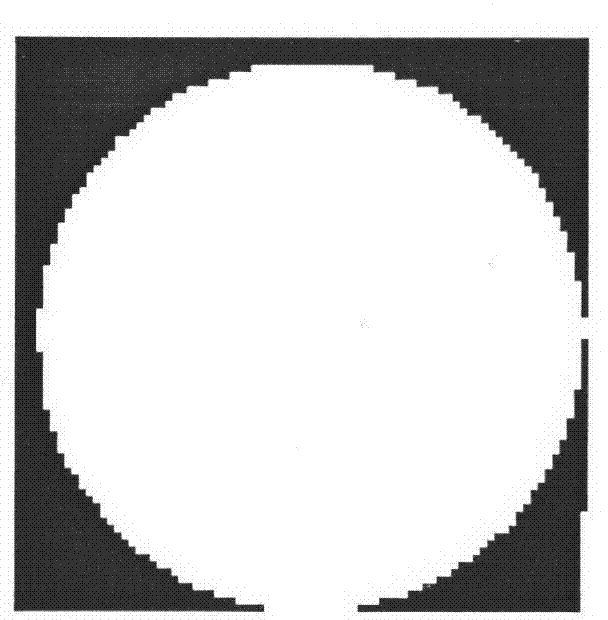
[0029] 1. Use the camera to capture the PCB image containing Mark points, and display it on the computer screen (called FOV field of view, FOV refers to the actual area currently captured by the camera), and then use the screenshot control that comes with the soldering robot to view the image in the current view. Intercept the area image contain...


PUM


Abstract

The invention discloses a method for locating Mark points on a PCB (printed circuit board) by utilizing an outline gravity center method. The method is characterized by comprising the following steps: on the basis of taking a Mark point extracted in initial programming as a datum point, taking the outline gravity center of the Mark point of the board to be detected, comparing the outline gravity center of the Mark point with the gravity center of the datum point, and performing PCB compensation by virtue of offset between the two gravity centers. The method is used for performing the PCB compensation by extracting the outline gravity center of the Mark point on the PCB and utilizing the offset between the gravity centers of the datum Mark point and the Mark point to be detected. The gravity centers are obtained by binary images and are easy and feasible to obtain. The algorithm is independent from the shapes of the Mark points, is not influenced by the intensity of illumination, achieves sub-pixel-level precision, and is high in compensation precision.

Description

technical field [0001] The invention relates to the field of visual detection of PCB welding, in particular to a method for locating Mark points of a PCB board by using a contour center-of-gravity method, so that the compensation accuracy can be effectively improved when positioning and correcting the PCB board. Background technique [0002] With the development of computer digital image processing technology and non-destructive testing technology, detection and recognition technology is increasingly developing towards intelligent, high-reliability, high-speed automatic online detection. Computer vision technology and reliability technology are the two major technical foundations of modern inspection. Machine vision has been successfully applied in the field of industrial inspection, including automatic inspection of PCB (printed circuit board), automatic positioning of circuit boards and calibration of benchmarks, which are important for accurate placement of components in ...

Claims


Application Information

Patent Timeline
Patent Type & Authority Applications(China)
IPC IPC(8): G06K9/32
Inventor 廖怀宝
Owner 廖怀宝
Why Eureka
Try Eureka