Method for manufacturing semiconductor device

A semiconductor and device technology, applied in the field of semiconductor device manufacturing, can solve problems such as inability to obtain high-quality SiGe, high etching speed, etc.

Active Publication Date: 2015-03-04
SEMICONDUCTOR MANUFACTURING INTERNATIONAL (BEIJING) CORP
View PDF3 Cites 0 Cited by
  • Summary
  • Abstract
  • Description
  • Claims
  • Application Information

AI Technical Summary

Problems solved by technology

[0008] However, since the etching rate in the crystal direction and the crystal direction is larger than that in the crystal direction, it often causes the flat bottom 260 of the groove 215 to be etched as Figure 2B pointed
However, if SiGe is epitaxially grown on the pointed bottom of groove 215, high-quality SiGe cannot be obtained.

Method used


Image

  • Method for manufacturing semiconductor device
  • Method for manufacturing semiconductor device
  • Method for manufacturing semiconductor device

Examples


Embodiment Construction

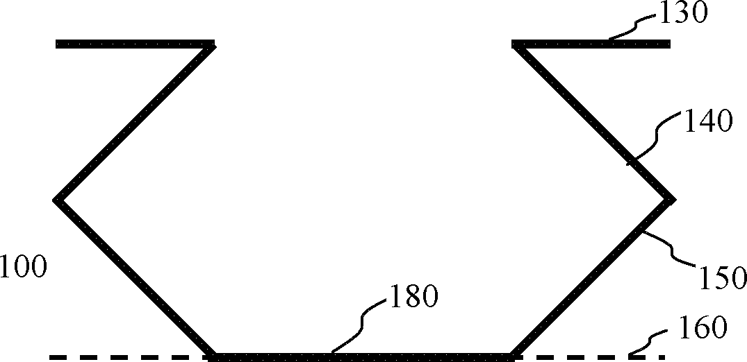
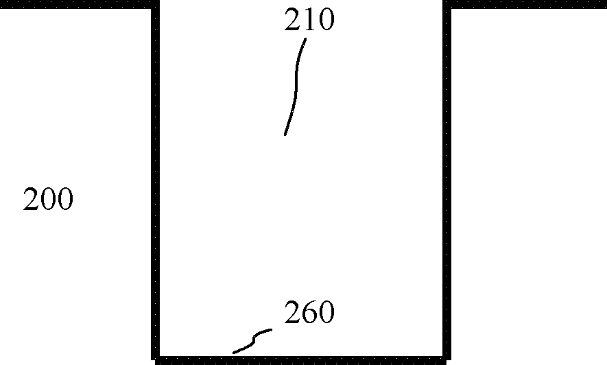
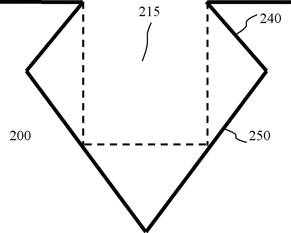
[0033] Various exemplary embodiments of the present invention will now be described in detail with reference to the accompanying drawings. It should be noted that the relative arrangements of components and steps, numerical expressions and numerical values ​​set forth in these embodiments do not limit the scope of the present invention unless specifically stated otherwise.

[0034] At the same time, it should be understood that, for the convenience of description, the sizes of the various parts shown in the drawings are not drawn according to the actual proportional relationship.

[0035] The following description of at least one exemplary embodiment is merely illustrative in nature and in no way taken as limiting the invention, its application or uses.

[0036] Techniques, methods and devices known to those of ordinary skill in the relevant art may not be discussed in detail, but where appropriate, such techniques, methods and devices should be considered part of the Authoriz...


PUM


Abstract

A method of fabricating a semiconductor device for improving the performance of "Sigma" shaped embedded source / drain regions is disclosed. A "U" shaped recess is formed in a Si substrate. The recess is treated with a surfactant, the amount of surfactant adsorbed on the recess sidewalls being greater than that on the recess bottom. An oxide is formed on the bottom. The presence of surfactant on the sidewalls, prevents oxide from forming thereon. The surfactant on the sidewalls is then removed and an orientation selective wet etching process is performed on the sidewalls. The oxide protects the Si at the bottom is from being etched.

Description

technical field [0001] The invention relates to a manufacturing method of a semiconductor device, in particular to a manufacturing method of a semiconductor device with a "Σ"-shaped embedded source and drain region. Background technique [0002] The development of semiconductor technology follows Moore's Law, and the critical dimensions are getting smaller and smaller. A technique of embedding silicon germanium (SiGe) in recessed source / drain regions to enhance channel mobility of PMOS devices has been proposed. Since the lattice constant of SiGe is larger than that of Si, it can provide compressive stress between the source and drain regions in the channel region of the PMOS device, thereby enhancing the hole mobility of the PMOS device. [0003] In order to enhance the effect of applying stress, a technical scheme of forming a "Σ"-shaped groove and filling it with SiGe is further proposed. [0004] figure 1 A "Σ" shaped groove formed in the substrate is schematically sh...

Claims


Application Information

Patent Timeline
Patent Type & Authority Patents(China)
IPC IPC(8): H01L21/336
CPCH01L21/3083H01L21/02238H01L29/7848H01L29/66636H01L21/30608
Inventor 刘焕新
Owner SEMICONDUCTOR MANUFACTURING INTERNATIONAL (BEIJING) CORP
Why Eureka
Try Eureka