A method for controlling the optical properties of synthesized perovskite by ion implantation technology

A technology of ion implantation and technology control, which is applied in the field of ion implantation technology to control the optical properties of perovskite after synthesis, which can solve problems such as difficult adjustment, and achieve the effect of improving basic research, broad application prospects, and simple methods

Inactive Publication Date: 2018-05-11
HARBIN INST OF TECH SHENZHEN GRADUATE SCHOOL
View PDF3 Cites 0 Cited by
  • Summary
  • Abstract
  • Description
  • Claims
  • Application Information

AI Technical Summary

Problems solved by technology

Once a lead halide perovskite device is synthesized, absorption and photoluminescence are fixed and difficult to tune

Method used


Image

  • A method for controlling the optical properties of synthesized perovskite by ion implantation technology
  • A method for controlling the optical properties of synthesized perovskite by ion implantation technology
  • A method for controlling the optical properties of synthesized perovskite by ion implantation technology

Examples


Embodiment 1

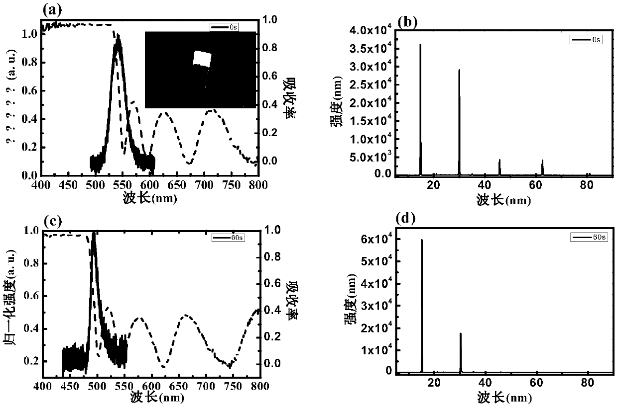
[0030] The first step in controlling the fluorescence and lasing emission of lead halide perovskites is to synthesize high-quality single-crystal perovskite microstructures. Here we synthesize CH 3 NH 3 PbBr 3 The perovskite is a one-step solution precipitation method commonly used in the prior art. This synthetic method can produce a large amount of high-quality CH 3 NH 3 PbBr 3 Microwires and Microblocks.

[0031]The size of the perovskite crystal microblocks we synthesized ranges from several microns to hundreds of microns in length, several microns to tens of microns in width, and hundreds of nanometers to several microns in thickness. The size of the perovskite microwire is several micrometers to tens of micrometers long, hundreds of nanometers to several micrometers wide, and hundreds of nanometers to several micrometers thick. In this example, we choose a micron block as an example to detail its corresponding optical properties. The corresponding scanning electr...

Embodiment 2

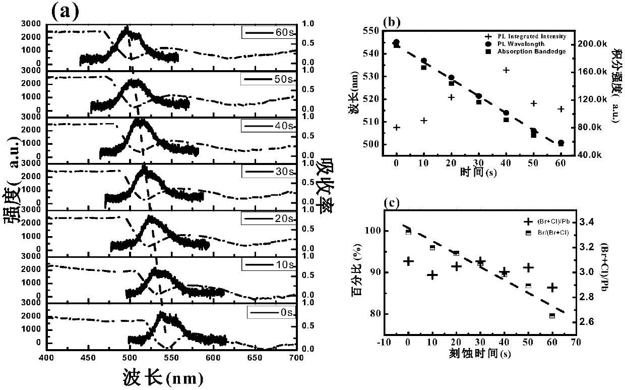
[0034] To confirm changes in chemical composition, we performed energy-dispersive X-ray spectroscopy (EDS) analysis. The ratio of Br / Pb in the as-grown perovskite is about 75 / 25, which is similar to that of PbBr 3 The stoichiometry matches. Then, the samples were etched in ICP chlorine gas for 60 s, the ratio of bromide / lead ions was changed to about 59.1 / 25, while the ratio of chloride / lead ions was increased from 0 to 15.2 / 25. figure 2 (c) represents the percentage of bromide and chloride ions in the perovskite microblocks as a function of etching time. Here all etching conditions are the same, as figure 2 As shown in (c), as the etching time increases, the ratio of (Br+Cl) / Pb remains basically unchanged, while the ratio of Br / (Br+Cl) decreases linearly. It shows that the bromide ion is decreasing and the chloride ion is increasing but their total amount remains unchanged. These results clearly demonstrate the behavior of chloride ions replacing bromide ions during etc...

Embodiment 3

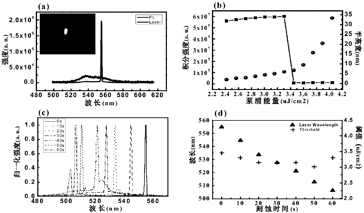
[0038] The most unique property of this technique of controlling the optical properties of as-synthesized perovskite crystals is that different locations of the same sample can be individually controlled, which is almost impossible in conventional solution processing techniques. To illustrate this advantage, we used electron beam lithography to etch another micron block and investigated the corresponding stimulated emission properties. A 300 nm e-beam resist of polymethyl methacrylate (PMMA) was spin-coated on the microblock and half the area was exposed with an e-beam. After developing in MIBK (Methyl Isobutyl Ketone, methyl isobutyl ketone), half of the microblock is still coated with polymethyl methacrylate and the other half is exposed to air, as Figure 4 The SEM image of the perovskite microblock is shown. The sample was then etched in the ICP for 30 seconds, Figure 5 Spectra obtained by pumping at different positions of perovskite microblocks half-covered with PMMA a...


PUM


Abstract

The invention provides a method for controlling an optical characteristic of perovskite after synthesis through ion implantation technology. The perovskite has a single-crystalline perovskite microstructure which comprises first halide ions. Ion implantation is performed on the single-crystalline perovskite microstructure according to an ion implantation method for a second halide, thereby realizing partial substitution of the first halide ions, wherein the second halide is different from the first halide. The method of the invention is advantageous in that simple preparation is realized; the ion implantation method can be used for selectively tuning photoluminescence and tuning lasing capability at different positions on one lead halide perovskite device; relatively simple experiment operation and relatively simple verification are realized; simple operation and high feasibility are realized; wide application prospect is obtained; and furthermore a new thought is supplied for development of a micro / nano optoelectronic field and a photonic device field.

Description

technical field [0001] The invention belongs to the technical field of photoelectric materials, and in particular relates to a method for controlling the optical properties of synthesized perovskite by ion implantation technology. Background technique [0002] The control of photoluminescence and absorption of lead halide perovskites plays a very critical role in the application of micro- and nano-sized light-emitting devices and photodetectors. Until now, wavelength control in lead halide perovskites was achieved by changing the halide mixture in solution. Once a lead halide perovskite device is synthesized, absorption and photoluminescence are fixed and difficult to tune. [0003] In the past two years, the lasing behavior of lead halide perovskite microwires and microblocks has been intensively studied. The relatively long carrier lifetime, diffusion length, and low defect density of single-crystal lead halide perovskites indicate very high optical gain and large extern...

Claims


Application Information

Patent Timeline
Patent Type & Authority Patents(China)
IPC IPC(8): H01J37/317H01L21/266
CPCH01J37/3171H01L21/266
Inventor 宋清海李建凯张楠张海涛肖淑敏
Owner HARBIN INST OF TECH SHENZHEN GRADUATE SCHOOL
Why Eureka
Try Eureka