
A display substrate, its manufacturing method, display panel and display device

A technology for a display substrate and a manufacturing method, applied in the fields of the manufacturing method, display substrate, display panel, and display device, capable of solving problems such as poor undercut of pixel electrodes and drain electrodes, reducing the risk of poor undercut, and improving product quality rate, to avoid the effect of holes

Inactive Publication Date: 2019-03-01
BOE TECH GRP CO LTD +1
View PDF8 Cites 0 Cited by
  • Summary
  • Abstract
  • Description
  • Claims
  • Application Information

AI Technical Summary

Problems solved by technology

[0004] The purpose of the embodiments of the present invention is to provide a display substrate, a manufacturing method thereof, a display panel and a display device, which are used to solve the undercut defect in the overlapping via hole between the pixel electrode and the drain electrode produced by the process in the prior art The problem

Method used


Image

  • A display substrate, its manufacturing method, display panel and display device
  • A display substrate, its manufacturing method, display panel and display device
  • A display substrate, its manufacturing method, display panel and display device

Examples


Embodiment Construction

[0027] A display substrate, a manufacturing method thereof, a display panel and a display device provided by the present invention will be described in more detail below with reference to the accompanying drawings and embodiments.

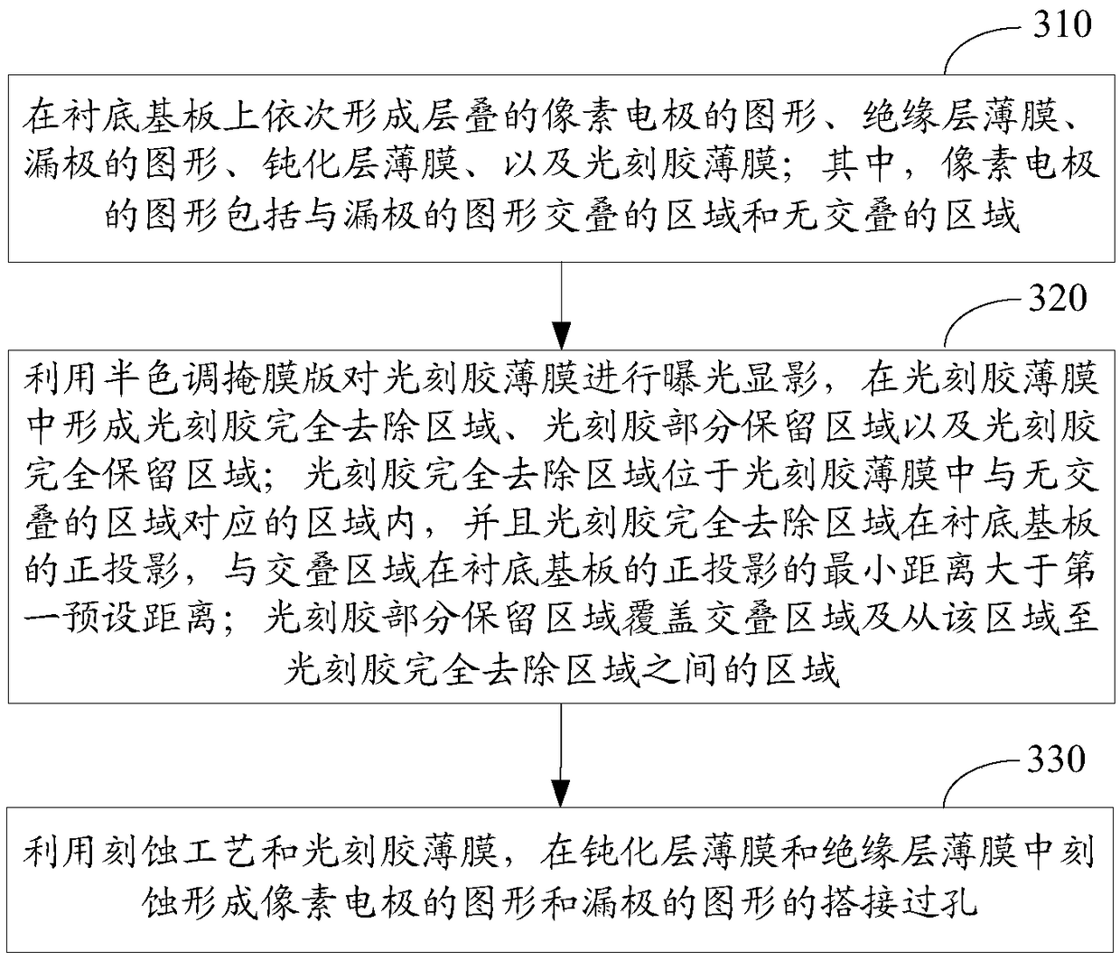
[0028] In an embodiment of the present invention, a method for manufacturing a display substrate is provided, such as image 3 As shown, at least the following steps are included:

[0029] Step 310, sequentially forming a layered pixel electrode pattern, an insulating layer film, a drain pattern, a passivation layer film, and a photoresist film on the base substrate; overlapping regions and non-overlapping regions.

[0030] Step 320, using a half-tone mask to expose and develop the photoresist film, forming a photoresist completely removed area, a photoresist partially reserved area, and a photoresist completely reserved area in the photoresist film; the photoresist is completely The removal area is located in the area corresponding to the above-...


PUM


Abstract

The embodiment of the invention discloses a display substrate, a manufacturing method of the display substrate, a display panel and a display device. In the scheme, as a certain distance exists between the complete removal zone in a photoresist film and the overlapping zone of a pattern of a pixel electrode and a pattern of a drain electrode in the display substrate manufacturing process, an etching range can not reach an insulating layer film corresponding to the overlapping zone of the pattern of the pixel electrode and the pattern of the drain electrode under limitation, a barrier effect is achieved, the insulating layer film in the zone is protected against etching, it is avoided that holes appear in the insulating layer film corresponding to the overlapping zone of the pattern of the pixel electrode and the pattern of the drain electrode, the risk of poor undercutting is lowered, and the product yield is increased.

Description

technical field [0001] The present invention relates to the field of display technology, in particular to a display substrate, a manufacturing method thereof, a display panel and a display device. Background technique [0002] Thin Film Transistor Liquid Crystal Display (TFT-LCD) has the characteristics of small size, low power consumption, and no radiation, and occupies a dominant position in the current flat panel display market. TFT-LCD mainly includes a liquid crystal display panel, a timing controller, and a driver integrated circuit (Integrated Circuit, IC). The display area on the array substrate is formed with a plurality of criss-cross gate lines and data lines, as well as a plurality of display units, each display unit corresponds to a TFT, and the TFT can control the inversion of the liquid crystal molecules in the corresponding display unit , so as to achieve the purpose of displaying the image. The driver IC of TFT-LCD includes source driver IC and gate driver...

Claims


Application Information

Patent Timeline
Patent Type & Authority Patents(China)
IPC IPC(8): H01L27/12H01L21/77G02F1/1362
CPCG02F1/136227G02F1/136295H01L27/1244H01L27/1259
Inventor 马涛林致远杨成绍
Owner BOE TECH GRP CO LTD
Learn More