Organic light emitting diode (OLED) display unit and OLED display device adopting display unit
A display unit and display module technology, applied in electrical components, electrical solid state devices, circuits, etc., can solve the problems of narrow packaging edge, high yield rate, wide distance between light-emitting pixels, etc., and achieve the effect of reducing packaging lines
- Summary
- Abstract
- Description
- Claims
- Application Information
AI Technical Summary
Problems solved by technology
Method used
Image
Examples
Embodiment
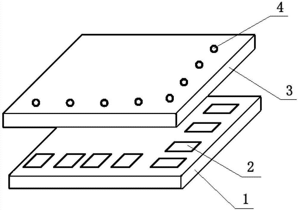
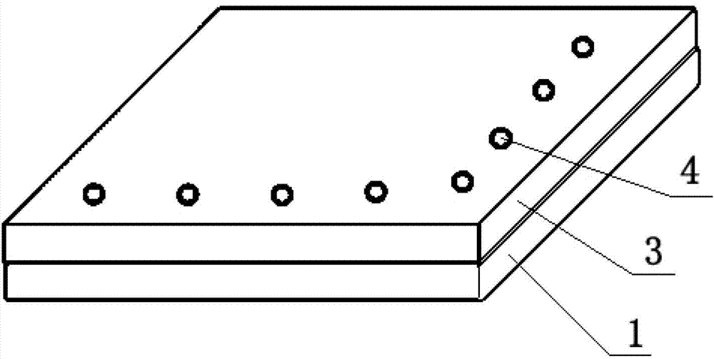
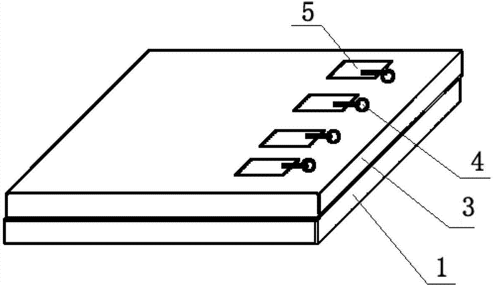
[0054] like Figure 1~Figure 3 As shown, the OLED display unit mainly includes two parts: a light-emitting device panel 1 and a packaging substrate 3. The light-emitting device panel 1 is provided with electrode terminals 2, and the positions on the packaging substrate 3 corresponding to the electrode terminals 2 are one-to-one. Through-holes 4 are processed, one side of the package substrate 3 is bonded to the side of the light-emitting device panel 1 provided with the electrode terminals 2, and the surroundings of the package substrate 3 and the light-emitting device panel 1 are bonded and packaged together. Conductive substances are poured into the through holes 4 and led to the other side of the packaging substrate 3 to form display unit electrodes 5, which are connected and connected to the electrode terminals 2 on the display substrate in one-to-one correspondence. The display unit electrodes 5 are used for Connect with drive control unit.
[0055] The light-emitting de...
manufacture Embodiment 1
[0063] Manufacturing steps process:
[0064] 1. Production of light-emitting device panel 1:
[0065] 1. Prepare an ITO glass substrate with an ITO matrix grid film layer including anode spacers and cathode spacers. The size is 96mm×96mm, and electrodes are respectively arranged on the two adjacent sides of the ITO glass substrate at right angles. Terminal 2, the OLED light-emitting device is fabricated on the ITO glass substrate of this specification.
[0066] 2. The RGB pixels of the light-emitting device panel 1 are produced by using the RGB metal mask alignment method, and the device structures of different colors of red, green and blue are as follows:
[0067] R pixel: ITO glass substrate / hole injection layer (thickness: 40nm; material: material of structural formula 4) / hole transport layer (thickness: 20nm; material: material of structural formula 5) / red light emitting layer (thickness: 30nm; material: structural formula 8 material, structural formula 5 material and st...
PUM
 Abstract
Description
Claims
Application Information


