

Low-insertion-loss coupling technique
A process method and chip technology, applied in the coupling of optical waveguides, etc., can solve the problems of hidden reliability, high price, and the accuracy of automatic search software cannot reach 100%, so as to avoid excessive loss and reduce production costs. Effect
- Summary
- Abstract
- Description
- Claims
- Application Information
AI Technical Summary
Problems solved by technology
Method used
Image

Examples
Embodiment 1
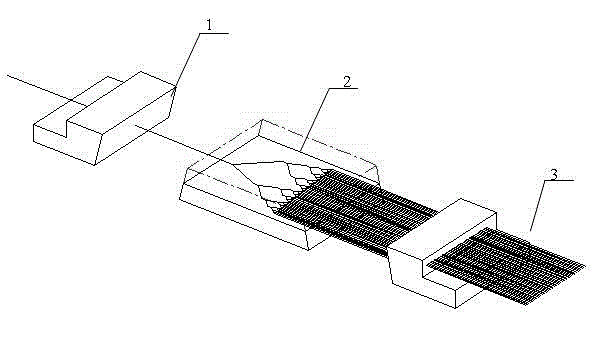
[0020] Such as figure 1 Shown:
[0021] Install the cleaned input single fiber 1 and planar waveguide chip 2 together with the fixtures on the six-dimensional adjustment frame in turn, and after finding the two side lines of the input single fiber 1 and planar waveguide chip 2 with the help of the microscopic observation system, first adjust the X axis to be parallel, and then Adjust the two sides on the Y axis to be parallel.
[0022] Turn on the light source, align the infrared light with the input single fiber 1 and the end face of the planar waveguide chip 2, hereinafter referred to as the coupling point, adjust the two light points refracted from the two ends by adjusting the knob, and then adjust the output end of the chip on the right side Place a mirror at the position, observe the corresponding channel light spot reflected by the channel at the output end of the chip, and find the brightest light spot by adjusting the coarse adjustment of the X and Y axes.
[0023] ...
PUM
 Abstract
Description
Claims
Application Information