Photoelectric device encapsulation and laser bonding temperature collection and control system and method

A technology of optoelectronic devices and control methods, applied in temperature control, control/regulation systems, non-electric variable control, etc., can solve the problem of lack of temperature acquisition and control modules, etc.

Inactive Publication Date: 2013-02-27
SHANGHAI UNIV
View PDF6 Cites 9 Cited by
  • Summary
  • Abstract
  • Description
  • Claims
  • Application Information

AI Technical Summary

Problems solved by technology

As for the impact of the temperature field on the packaging quality of OLED devices during laser bonding, there have been many data simulations. ANSYS is used for simulation experiments, but there is no temperature acquisition and control module in the real experiments.

Method used


Image

  • Photoelectric device encapsulation and laser bonding temperature collection and control system and method
  • Photoelectric device encapsulation and laser bonding temperature collection and control system and method
  • Photoelectric device encapsulation and laser bonding temperature collection and control system and method

Examples


Embodiment 1

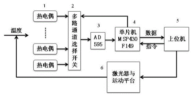
[0040] see figure 1, the photoelectric device packaging, laser bonding temperature acquisition and control system, including K-type thermocouple (1), analog switch CD4051 (2), temperature conversion chip AD595 (3), single-chip MSP430F149 (4), host computer (5 ), a laser and a motion platform (6), characterized in that: the K-type thermocouple (1) is connected to the single-chip microcomputer MSP430F149 (4) through the analog conversion switch CD4051 (2) through the temperature conversion chip AD595 (3); the single-chip microcomputer MSP430F149 (4) Connect and feedback control the analog switch CD4051 (2), and connect with the host computer (5), and the host computer (5) controls the bonding by controlling the laser and the motion platform (6) through its control program temperature.

Embodiment 2

[0042] see figure 1 , the optoelectronic device packaging, laser bonding temperature acquisition control system, including 8-way K-type thermocouple (1), multi-channel selection switch (2), AD595 chip (3), single-chip MSP430F149 (4), upper computer (5 ), laser and motion platform (6).

Embodiment 3

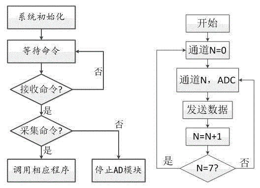
[0044] The optoelectronic device packaging, laser bonding temperature acquisition and control method, using the above system to operate, the operation steps:

[0045] 1. Place the OLED device to be packaged on the fixture platform for alignment and fixation;

[0046] 2. The upper computer (5) sends commands to run the laser and the motion platform (6) to make the laser head move according to the specified

[0047] Laser encapsulation of OLED devices;

[0048] 3. The upper computer and the lower computer carry out data transmission and communication, and send control commands from the upper computer to the unit.

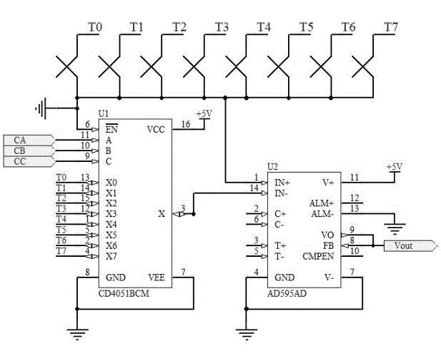
[0049] In the MSP430F149 (4), the MSP430F149 (4) executes the command to control the multi-channel selection switch (2) to collect the temperature signals of the 8 thermocouples in sequence;

[0050] 4. Amplify and condition the collected temperature analog signal through AD595 (3) and then transmit it to

[0051] Input to the MSP430F149 (4) for analog-to-digital c...


PUM


Abstract

The invention relates to a photoelectric device encapsulation and laser bonding temperature collection and control system and method. The laser bonding encapsulation adopts K-type thermocouple to collect the temperature. Collected temperature signals are selected by a multipath channel selector switch before AD (analogue-digital) conversion; converted signals are led into a single chip MSP430F149 for processing; and processed data is transmitted to an upper computer for communication and control to automatically regulate the power of laser or the scanning speed of a laser head so as to stabilize the temperature in a laser bonding process of a glass material within a certain range. The control system is mainly applied to photoelectric devices such as organic light-emitting diode (OLED) displays and MEMS (micro-electro-mechanical systems) encapsulated by the glass material, taking the OLED devices as an example for exposition.

Description

technical field [0001] The invention relates to a photoelectric device packaging, laser bonding temperature acquisition and control system and method. Background technique [0002] OLED (Organic Light Emitting Diode) display technology has been valued due to its excellent luminous performance and wide application prospects. OLED has the advantages of high brightness, good color contrast, wide viewing angle, fast refresh rate and low energy consumption. However, the organic light-emitting layer and electrodes in the OLED device are very sensitive to oxygen and moisture in the surrounding environment, and will interact with it to degrade, thus greatly affecting the service life of the OLED device. The lifespan of the device can be significantly extended by separating the organic light-emitting layer and the electrode in the OLED device from the surrounding environment in a hermetic sealing manner. [0003] The uneven temperature field during laser bonding has a great impact...

Claims


Application Information

Patent Timeline
Patent Type & Authority Applications(China)
IPC IPC(8): G05D23/22
Inventor 赖禹能葛军锋张建华黄元昊陈遵淼
Owner SHANGHAI UNIV
Why Eureka
Try Eureka