
Through hole structure, printed circuit board, and manufacture method of through hole structure

A technology of printed circuit substrate and manufacturing method, which is applied in the directions of printed circuit components, electrical connection formation of printed components, electrical connection of printed components, etc., can solve the problems of poor product reliability, high manufacturing difficulty and high production cost, and achieves reduction of hole thickness. diameter ratio, reducing the difficulty of PCB manufacturing, improving processing efficiency and yield

Active Publication Date: 2013-02-27
XFUSION DIGITAL TECH CO LTD
View PDF4 Cites 32 Cited by
  • Summary
  • Abstract
  • Description
  • Claims
  • Application Information

AI Technical Summary

Problems solved by technology

However, the process is complicated, the manufacturing is difficult, the production cost is high, and due to factors such as easy accumulation of liquid medicine in blind holes, the reliability of the product is poor and the yield rate is low

Method used


Image

  • Through hole structure, printed circuit board, and manufacture method of through hole structure
  • Through hole structure, printed circuit board, and manufacture method of through hole structure
  • Through hole structure, printed circuit board, and manufacture method of through hole structure

Examples


Embodiment Construction

[0060] The following will clearly and completely describe the technical solutions in the embodiments of the present invention with reference to the accompanying drawings in the embodiments of the present invention. Obviously, the described embodiments are only some, not all, embodiments of the present invention. Based on the embodiments of the present invention, all other embodiments obtained by persons of ordinary skill in the art without making creative efforts belong to the protection scope of the present invention.

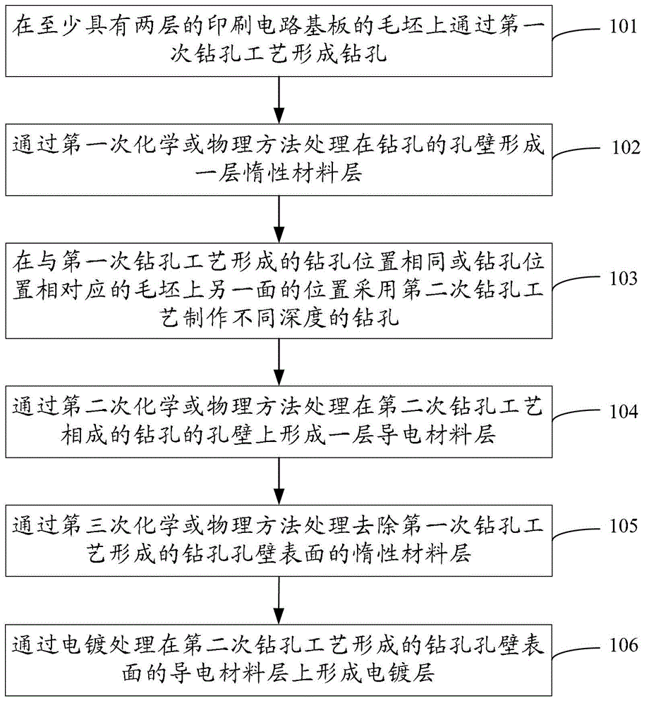
[0061] refer to figure 1 As shown, the embodiment of the present invention provides a method for manufacturing a through-hole structure, including the following steps:

[0062] 101. Form a drill hole 1 on a blank of a printed circuit substrate having at least two layers by a first drilling process.

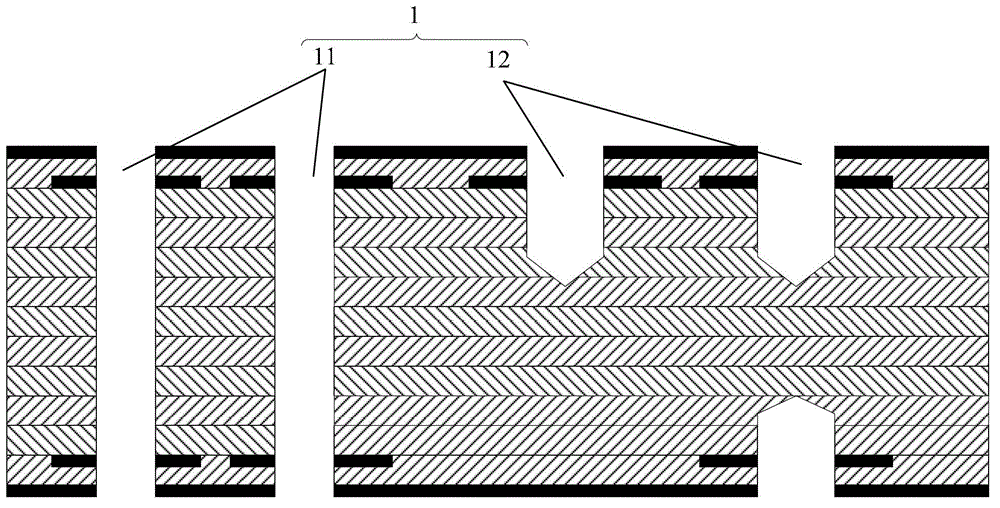
[0063] The borehole 1 described here includes a through hole 11 or a blind hole 12, wherein the borehole diameter and the borehole depth are determined by the pr...


PUM


Abstract

The embodiment of the invention provides a through hole structure, a printed circuit board and a manufacture method of the through hole structure, and relates to the field of printed circuit boards. According to the invention, the density of an outgoing line is increased, the transmission capacity of a signal is increased, the manufacture difficulty is lowered, and the product reliability is improved. The through hole structure is surrounded by hole walls and comprises at least two through hole parts which are formed through division along the axial direction of the through hole structure and at least one step part which is formed through division along the axial direction, wherein the at least two through hole parts are surrounded by the hole walls, the at least one step part is surrounded by the hole walls, each step part of the at least one step part is located between two adjacent through hole parts of the at least two through hole parts and is connected with the two adjacent through hole parts; and the hole walls of the at least two through hole parts and the hole walls of the at least one step part at least comprise one insulated hole wall and one metalized hole wall. The example of the invention is applied to manufacturing the printed circuit board.

Description

technical field [0001] The invention relates to the field of printed circuit substrates, in particular to a through-hole structure, a printed circuit substrate and a method for manufacturing the through-hole structure. Background technique [0002] With the rapid development of network products, the channel capacity of the backplane (Backplane) is expanding. At present, the use of ordinary through-hole technology makes the printed circuit board (Printed Circuit Board, referred to as "PCB") design layers and board thickness higher and higher, and the size design is larger and larger, thus improving the manufacturing process of printed circuit boards. It has brought great challenges, which are mainly reflected in the fact that the number of layers, size, board thickness, and through-hole plating capacity of the printed circuit board have reached the capability limit of the manufacturer's equipment. Therefore, the room for improving the signal transmission capacity of the syst...

Claims


Application Information

Patent Timeline
Patent Type & Authority Applications(China)
IPC IPC(8): H05K3/42H05K1/11
Inventor 刘山当高峰周水平
Owner XFUSION DIGITAL TECH CO LTD
Learn More