Welding process of plug-in unit of PCB (Printed Circuit Board)

A technology of PCB board and welding process, which is applied in the field of PCB board plug-in welding process, can solve problems such as low safety, increase the probability of bad solder joints, and affect cutting, so as to strengthen employee safety protection, facilitate board insertion operations, Effect of reducing solder loss

Inactive Publication Date: 2013-03-06
QIXIANG ELECTRON SCI & TECH
View PDF5 Cites 9 Cited by
  • Summary
  • Abstract
  • Description
  • Claims
  • Application Information

AI Technical Summary

Problems solved by technology

[0004] 1), the components are long, the plug-in speed is slow, and the efficiency is low;
[0005] 2), manual dip soldering, the operation requires certain skills, and the production efficiency is low; manual work, easy to fatigue, low safety; product quality is not easy to guarantee, there are more residues, and the production quality is low;
[0006] 3) To cut the feet, usually use a saw disc cutting machine, which has high noise, low safety performance (lack of protection, easy to hurt hands), low production efficiency, and often needs auxiliary scissors to cut the feet, and the production efficiency is especially low;
[0007] 4) Due to the long legs of the component, often due to the too close spacing of the legs, a large tin block will be formed after passing the tin, which will affect the cutting and even damage the cutting machine;
[0008] 5) Due to the push and pull force during cutting, tiny cracks will form between the solder of most of the solder joints and the part feet, resulting in certain hidden dangers in the quality of the products;
[0009] 6), the above process increases the probability of bad solder joints, increases the workload of repair welding work, and affects production efficiency;
[0010] 7) The legs of the cut-off components are all stained with a lot of solder, resulting in excessive loss of solder, resulting in a certain cost waste

Method used


Image

  • Welding process of plug-in unit of PCB (Printed Circuit Board)

Examples


Embodiment Construction

[0030] The present invention will be further described in conjunction with the accompanying drawings and specific embodiments.

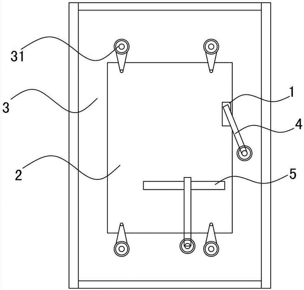
[0031] refer to figure 1 , a kind of PCB board plug-in welding process of the present invention, described process comprises the steps:

[0032] (1) Cutting the feet of components, using an automatic cutting machine to trim the feet of components to uniform and standardized specifications, and obtain short-leg components of uniform specifications 1;

[0033] (2), plug-in, first put the PCB board 2 to be processed into the limit groove of the wave soldering machine tray 3, and then fix the PCB board 2 on the tray 3 with the four fixing buckles 31 on the tray 3, and then put the upper The components 1 processed in one step are respectively inserted into the corresponding pads of the PCB board 2 mounted on the tray 3 of the wave soldering machine;

[0034] (3), check and press the parts, visually confirm that each component 1 is inserted correctly, an...


PUM


Abstract

The invention relates to the technical field of welding of a PCB (Printed Circuit Board), and provides a welding process of a plug-in unit of the PCB, which can effectively improve the production efficiency, improves the production quality, reduces the production loss and cost, and reduces the operation difficulty and human errors. The process comprises the following steps of: (1) trimming supporting legs of components: trimming the supporting legs of the components into union and formal specification; (2) inserting the components: respectively the components processed in step (1) into corresponding welding pads of the PCB on a tray of a wave soldering machine; (3) viewing and pressing the components: performing visual inspection to confirm that the components are correctly inserted, and then pressing the components on the PCB; (4) performing wave soldering welding: performing welding operation on the PCB by the wave soldering machine; (5) taking out the PCB: taking out the PCB from the tray of the wave soldering machine; (6) detection: detecting the welding quality of the PCB, if the welding quality is qualified, obtaining the finished product, and if the welding quality is disqualified, performing the next step on the disqualified product; and (7) repairing welding: performing manual repairing welding operation on detected poor welding points of the PCB, and obtaining the finished product.

Description

technical field [0001] The invention relates to the technical field of PCB board welding, in particular to a PCB board plug-in welding process. Background technique [0002] At present, the wave soldering process is usually used for soldering plug-ins on PCB boards, and the process is as follows: plug-in-inspection-dip soldering-cutting feet-taking board-testing-repair soldering-finishing; that is, the components are first Insert the PCB board, then check visually to confirm that the components are inserted in place, then perform soldering operations with manual dip soldering, and then use a sawing machine to cut the long legs of the components soldered on the PCB board, and cut the PCB board from Take it out from the tray, conduct quality inspection on the soldered PCB board, correct some bad solder joints by manual welding, and finally get the finished product. [0003] This welding process has the following problems: [0004] 1), the components are long, the plug-in spe...

Claims


Application Information

Patent Timeline
Patent Type & Authority Applications(China)
IPC IPC(8): B23K1/00B23K1/20B23K3/08
Inventor 吴怀升郭玉宗钟理治徐泽山赖章波
Owner QIXIANG ELECTRON SCI & TECH
Why Eureka
Try Eureka