
UV transfer printing in-mold-transfer printing decoration method

A technology of transferring molds and molds, applied in the direction of coating, etc., can solve problems such as failure to meet high and low temperature limit tests, product deformation, and easy flushing of ink at the injection molding inlet

Inactive Publication Date: 2013-03-06
东莞市崇康电子有限公司
View PDF5 Cites 16 Cited by
  • Summary
  • Abstract
  • Description
  • Claims
  • Application Information

AI Technical Summary

Problems solved by technology

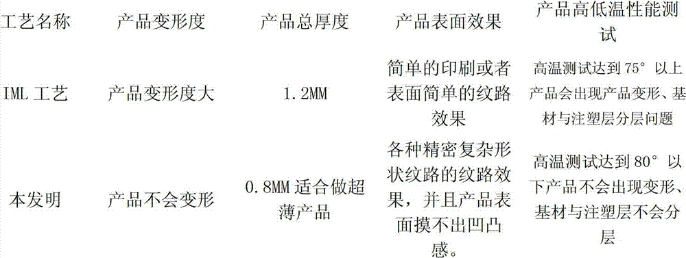
[0006] 1. Ultra-thin products cannot be satisfied, and the overall thickness requirement is greater than 1.2MM. Products thinner than this thickness are easy to flush ink at the injection molding inlet
[0007] 2. Unable to meet the high and low temperature limit test, the product is seriously deformed when the product is tested for high and low temperature limit
[0008] 3. When the product is subjected to high and low temperature limit tests, the product will have delamination between the printing layer and the injection layer

Method used


Image

  • UV transfer printing in-mold-transfer printing decoration method
  • UV transfer printing in-mold-transfer printing decoration method

Examples


Embodiment 1

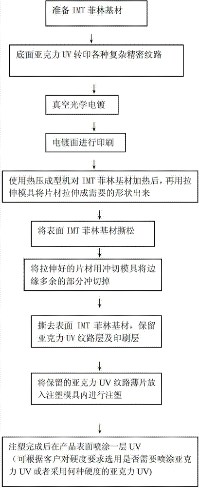
[0036] A UV transfer printing in-mold transfer decoration method is characterized in that it comprises the following steps:

[0037] (1) Prepare the IMT film, and make acrylic UV texture molding on the other side of the non-PET diaphragm of the film material;

[0038] (2) Put the IMT film with the formed pattern into the vacuum optical plating equipment, and the electroplating increases the transparent plating or color plating;

[0039] (3) Put the printed IMT film on the hot-pressing mold, heat it with a hot press, and stretch it into the shape required by the customer;

[0040] (4) Use a stamping die to punch off the excess part of the edge of the stretched IMT film sheet;

[0041] (5) Tear off the IMT film PET protective film on the surface of the die-cut sheet, leaving only the acrylic UV layer and the printing layer;

[0042] (6) Put it into the injection mold for injection molding.

Embodiment 2

[0044] Use the UV transfer printing in-mold transfer printing decoration method of the present invention on the mobile phone shell, wherein the shell of the mobile phone is made of ABS / ABS+PC / PC material. The IMT film mentioned above is a raw material, which needs to be torn off before final injection molding. The process is shown in Figure 1, and the steps are as follows:

[0045] 1. Prepare the IMT film, and make acrylic UV pattern forming on the other side of the non-PET diaphragm of the film material.

[0046] Take the desired texture effect mold, pour acrylic glue on the mold, then take the IMT film non-PET film and put it on the mold, use the dust roller to flatten the acrylic back and forth on the film, and then put the mold into the UV tunnel Use a UV lamp to light-cure the acrylic. After light-curing, tear off the IMT film from the mold. The total thickness of the lines is 0.001-0.005MM, the peak energy of UV light-curing is 400-1000MJ, and the light-curing time is 3...

Embodiment 3

[0055] Use the UV transfer printing in-mold transfer printing decoration method of the present invention on the palmtop computer shell, and the shell of the palmtop computer is made of ABS material. The IMT film mentioned above is a raw material, which needs to be torn off before final injection molding.

[0056] The process steps are as follows:

[0057] 1. Prepare the IMT film, and make acrylic UV pattern forming on the other side of the non-PET diaphragm of the film material.

[0058] Take the desired texture effect mold, pour acrylic glue on the mold, then take the IMT film non-PET film and put it on the mold, use the dust roller to flatten the acrylic back and forth on the film, and then put the mold into the UV tunnel The acrylic is light-cured with a UV lamp. After light-curing, the IMT film is torn off from the mold. The total thickness of the lines is 0.003MM, the peak energy of UV light-curing is 1200MJ, and the light-curing time is 4 seconds.

[0059] 2. Put the I...


PUM

PropertyMeasurementUnit
thicknessaaaaaaaaaa
thicknessaaaaaaaaaa
thicknessaaaaaaaaaa

Abstract

The present invention belongs to a process for electronic and electrical appliance shell surface treatment, and specifically relates to a UV transfer printing in-mold-transfer printing decoration method, which comprises the following steps: (1) preparing an IMT film, and carrying out acrylic UV line forming on the other surface of the film material non-PET diaphragm; (2) placing the line-formed IMT film in a vacuum optical electroplating device, and carrying out electroplating to increase transparent plating or color plating; (3) placing the printed IMT film on a hot pressing mold to heat and stretch into a shape required by a customer by using a hot pressing machine; (4) adopting a stamping mold to stamp the redundant part on the edge of the stretched IMT film sheet material; (5) peeling the IMT film PET protection film on the surface of the stamped sheet material to only leave the acrylic UV layer and the printing layer; and (6) placing in an injection mold to carry out injection molding. According to the UV transfer printing in-mold-transfer printing decoration method, the surface of the product is the ultra-thin acrylic UV, and can bear a high temperature (350 DEG C) injection molding material during injection molding, ink can not punch through the glue inlet during injection molding, the ultra-thin product can be produced, and problems of product deformation, layering and the like can be solved when temperature limit testing is performed.

Description

technical field [0001] The invention belongs to a process for surface treatment of shells of electronic and electrical appliances, and in particular relates to a UV transfer printing in-mold transfer decoration method. Background technique [0002] IML technology: Chinese name: in-mold decoration technology, also known as coating-free technology. English name: In-Mold Decoration, IMD is an internationally popular surface decoration technology. The surface is hardened transparent film, the middle printing pattern layer, the back injection molding layer, and the middle of the ink, which can make the product resistant to friction, prevent the surface from being scratched, and can last for a long time. Keep the color bright and not easy to fade. [0003] Existing IML process steps: [0004] Material cutting---flat printing---ink drying and fixing---sticking protective film---punching positioning hole---thermoforming---cutting peripheral shape---material injection molding. The...

Claims


Application Information

Patent Timeline
Patent Type & Authority Applications(China)
IPC IPC(8): B29C45/14
Inventor 全峻成
Owner 东莞市崇康电子有限公司
Learn More