
Chamber device and substrate treating plant with same

A substrate processing equipment and chamber technology, applied in the field of microelectronics, can solve the problems of inability to ensure the uniformity of the temperature field of the tray, uneven heating of the tray, large radial temperature difference of the tray, etc., so as to reduce the radial temperature difference and achieve uniform heating. , to ensure the effect of uniformity

Inactive Publication Date: 2013-03-06
BEIJING NAURA MICROELECTRONICS EQUIP CO LTD
View PDF3 Cites 7 Cited by
  • Summary
  • Abstract
  • Description
  • Claims
  • Application Information

AI Technical Summary

Problems solved by technology

[0004] Traditional MOCVD equipment has a layer of trays placed inside the reaction chamber, and the efficiency of substrate processing is low
In addition, the heating of the tray is not uniform, that is, the radial temperature difference of the tray is large, so the uniformity of the temperature field of the tray cannot be guaranteed

Method used


Image

  • Chamber device and substrate treating plant with same

Examples


Embodiment Construction

[0025] Embodiments of the present invention are described in detail below, examples of which are shown in the drawings, wherein the same or similar reference numerals designate the same or similar elements or elements having the same or similar functions throughout. The embodiments described below by referring to the figures are exemplary only for explaining the present invention and should not be construed as limiting the present invention.

[0026] In describing the present invention, it is to be understood that the terms "upper", "lower", "front", "rear", "top", "bottom", "inner", "outer" etc. indicate an orientation or position The relationship is based on the orientation or positional relationship shown in the drawings, and is only for the convenience of describing the present invention and simplifying the description, rather than indicating or implying that the referred device or element must have a specific orientation, be constructed and operated in a specific orientati...


PUM


Abstract

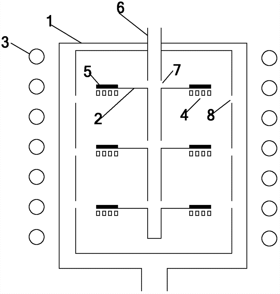
The invention discloses a chamber device which comprises a chamber body, a tray, an external heating source and an auxiliary heating source, wherein a chamber is defined in the chamber body; the tray is arranged in the chamber and used for carrying a substrate; the external heating source is arranged around the periphery of the chamber body; and the auxiliary heating source is arranged on the tray and used for heating the tray. The chamber device disclosed by the embodiment of the invention adopts the external heating source and the auxiliary heating source for common heating, and can compensate uneven temperature distribution on the tray to reduce the radial temperature difference on the tray, thereby ensuring the evenness of the temperature field; and thus, the invention has the advantages of even substrate heating and high treatment efficiency. The invention also discloses a substrate treating plant with the chamber device.

Description

technical field [0001] The invention relates to the technical field of microelectronics, in particular to a chamber device and substrate processing equipment with the chamber device. Background technique [0002] Metal organic compound vapor deposition (MOCVD) is a new technology of compound semiconductor vapor phase epitaxy developed in the 1960s that uses metal organic compounds for metal transport. This technology can precisely control the thickness and composition of the epitaxial layer at the nanoscale. , and is suitable for mass production, it has become the main production method of optoelectronic devices. [0003] MOCVD equipment is mainly composed of the following subsystems: (1) reaction chamber subsystem; (2) gas transport subsystem; (3) exhaust gas treatment subsystem, as shown in Figure 2. Among them, the reaction chamber subsystem is the core component of MOCVD equipment, and its design scheme has a decisive impact on the quality of the epitaxial layer and the...

Claims


Application Information

Patent Timeline
IPC IPC(8): C23C16/46C23C16/18
Inventor 王一帆
Owner BEIJING NAURA MICROELECTRONICS EQUIP CO LTD
Learn More