

Semiconductor power conversion device
A power conversion device and power conversion technology, applied in the direction of output power conversion device, AC power input conversion to DC power output, electrical components, etc., can solve the problem of thermal damage of semiconductor components, achieve uniform temperature rise and prevent damage Effect
- Summary
- Abstract
- Description
- Claims
- Application Information
AI Technical Summary
Problems solved by technology
Method used
Image

Examples
Embodiment approach 1
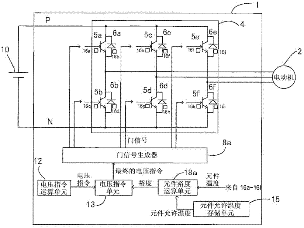
[0026] figure 1 It is a figure which shows the structure of the semiconductor power conversion device in Embodiment 1 of this invention. exist figure 1 Among them, the reference number 1 is a semiconductor power conversion device, the reference number 10 is a DC power supply device connected between the P-side bus bar and the N-side bus bar of the semiconductor power conversion device, and the number 2 is the three-phase voltage output from the semiconductor power conversion device 1. driven motor. In addition, the DC power supply device 10 may be a power supply obtained by rectifying and smoothing an AC power supply. In addition, the motor 2 may be any of an induction motor, a permanent magnet motor, and the like, and any type of motor may be used.
[0027] In addition, reference numerals 5a to 5f are U-phase, V-phase, and W-phase P-side and N-side semiconductor switching elements, which are switched on or off by a gate signal from the gate signal generator 8a, thereby swi...
Embodiment approach 2
[0047] Figure 10 It is a figure which shows the structure of the semiconductor power conversion device in Embodiment 2 of this invention. Additionally, for figure 1 The same structures are marked with the same symbols, and their descriptions are omitted. use Figure 10 , the operation according to the embodiment of the present invention will be described.
[0048] exist Figure 10 , the gate signal generator 8b performs AND figure 1 The same operation as the gate signal generator 8a, for example, by comparing the magnitude of a carrier waveform such as a triangle wave with a voltage command, and generating a gate signal (gate on signal) that turns on the semiconductor switching element when the voltage command is greater than the carrier waveform , when the voltage command is smaller than the carrier waveform, a gate signal (gate off signal) for turning off the semiconductor switching element is generated. and figure 1 The gate signal generator 8a differs in that it ou...
Embodiment approach 3
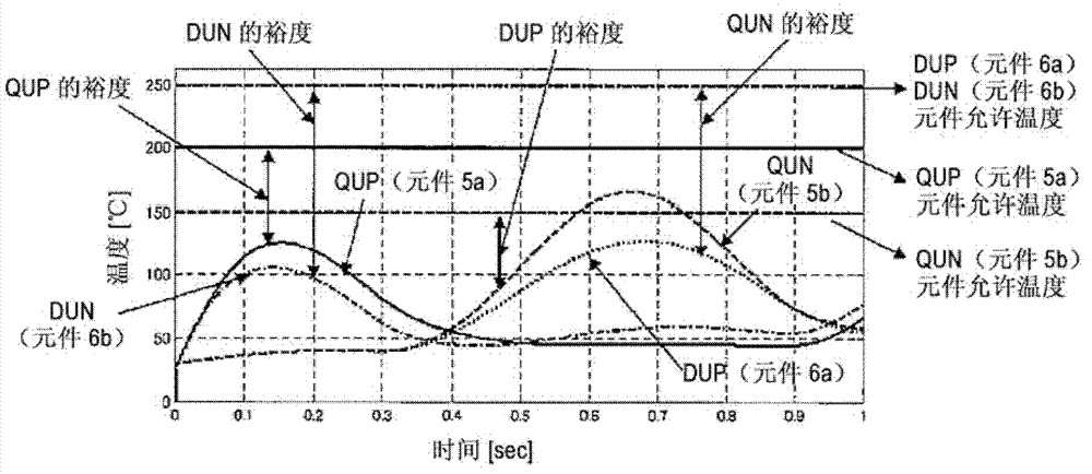
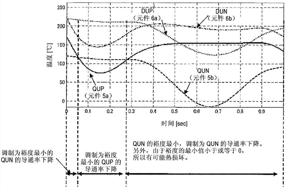
[0053] Figure 11 It is a figure which shows an example of the structure of the semiconductor power conversion device in Embodiment 3 of this invention. Additionally, for figure 1 and Figure 10 The same structures are marked with the same symbols, and their descriptions are omitted. use Figure 11 , the operation according to the embodiment of the present invention will be described.
[0054] The element temperature detectors 16a and 16b are element temperature detectors that detect the element temperatures of the semiconductor switching element 5a and the semiconductor element 6a, respectively. As the structure of this element temperature detector, for example, a member capable of detecting the temperature of the semiconductor element such as a thermocouple is bonded to the vicinity of the semiconductor switching element and the semiconductor element, or a temperature detector is built in the semiconductor switching element and the semiconductor element. Components with...
PUM
 Abstract
Description
Claims
Application Information