Packaging structure of organic light emitting diode

A technology of light-emitting diodes and packaging structures, which is applied in the manufacture of electrical components, electrical solid devices, semiconductor/solid devices, etc. It can solve problems such as the inability of adhesive materials to block water vapor and damage to OLED devices, so as to isolate damage and improve the ability to prevent , the effect of reducing damage

Inactive Publication Date: 2013-03-20
AU OPTRONICS CORP
View PDF0 Cites 22 Cited by
  • Summary
  • Abstract
  • Description
  • Claims
  • Application Information

AI Technical Summary

Problems solved by technology

However, since the adhesive material cannot block water vapor, water vapor can easily enter the OLED device from the side of the frame glue, causing damage to the OLED device

Method used


Image

  • Packaging structure of organic light emitting diode
  • Packaging structure of organic light emitting diode
  • Packaging structure of organic light emitting diode

Examples


Embodiment Construction

[0035] In order to make the technical content disclosed in this application more detailed and complete, reference may be made to the drawings and the following various specific embodiments of the present invention, and the same symbols in the drawings represent the same or similar components. However, those skilled in the art should understand that the examples provided below are not intended to limit the scope of the present invention. In addition, the drawings are only for schematic illustration and are not drawn according to their original scale.

[0036] The specific implementation manners of various aspects of the present invention will be further described in detail below with reference to the accompanying drawings.

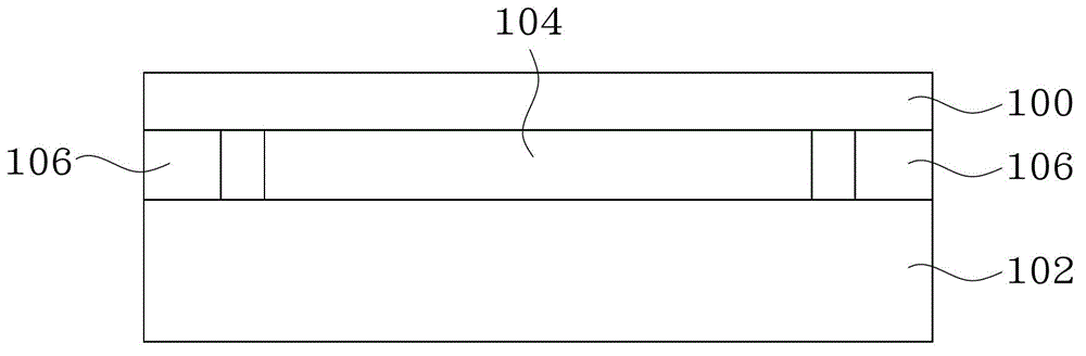
[0037] figure 1 A schematic diagram showing the composition of an organic light emitting diode packaging structure in the prior art.

[0038] refer to figure 1 , the organic light emitting diode packaging structure includes a glass substrate 102 , an org...


PUM


Abstract

The invention provides a packaging structure of an OLED (organic light emitting diode), which comprises a substrate, an OLED device, an air-barrier film and a metal packaging film, wherein the OLED device is arranged above the substrate; the air-barrier film is positioned above the OLED device; the OLED device is covered with the air-barrier film; the air-barrier film is glued to the substrate by virtue of a seal to form an enclosed space for sealing the OLED device; and the metal packaging film is arranged in a neighbor area where the substrate is glued with the air-barrier film, so that external moisture is prevented from entering the enclosed space. Compared with the prior art, after the air-barrier film is glued with the substrate, the metal packaging film is coated in the seal neighbor area in a sputter or evaporation coating mode at the side edges of the air-barrier film and the seal, the damage of the external moisture to the OLED device is thoroughly isolated by the metal packaging film, the stopping capacity of the packaging structure to the moisture is improved, and moisture absorption layers can be coated on the two sides of the OLED device before the seal is coated, thereby reducing the damage of the moisture in a glue material to the OLED device during coating.

Description

technical field [0001] The invention relates to an organic light emitting diode, in particular to the packaging structure of the organic light emitting diode. Background technique [0002] Organic Light Emitting Diode (OLED) panel is a display element with high brightness, high response speed, thin and short, full color, no viewing angle difference and no backlight, so it has taken the lead in replacing TN (Twisted Nematic, twisted nematic) liquid crystal panel market, and will further pose a market threat to small-sized thin film transistor liquid crystal display devices (Thin Film Transistor Liquid Crystal Display, TFT-LCD). Currently, OLED panels have been applied to the display screens of portable digital products such as mobile phones, personal digital assistants and even notebook computers. [0003] Generally speaking, OLED panels can be classified into top emission, bottom emission or double emission. It is mainly due to the difference in the selection of light-emit...

Claims


Application Information

Patent Timeline
Patent Type & Authority Applications(China)
IPC IPC(8): H01L51/50H01L51/52
Inventor 王铮亮洪仕馨
Owner AU OPTRONICS CORP
Why Eureka
Try Eureka