Radio-frequency filter piece packaging structure
A technology of device packaging and radio frequency filtering, which is applied in the field of integrated circuits, can solve the problems of difficult adjustment of inductance value and large space occupied by inductors, and achieve the effect of low cost and cost saving
- Summary
- Abstract
- Description
- Claims
- Application Information
AI Technical Summary
Problems solved by technology
Method used
Image
Examples
Embodiment Construction
[0027] Exemplary embodiments of the present invention are described below in conjunction with the accompanying drawings, which include various details of the embodiments of the present invention to facilitate understanding, and they should be regarded as exemplary only. Accordingly, those of ordinary skill in the art will recognize that various changes and modifications of the embodiments described herein can be made without departing from the scope and spirit of the invention. Also, descriptions of well-known functions and constructions are omitted in the following description for clarity and conciseness.
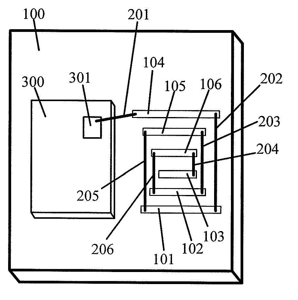
[0028] image 3 is a schematic diagram of a chip package structure according to an embodiment of the present invention. As shown in the figure, a bonding area 301 is provided on the die 300 adhered to the surface of the packaging substrate 100 by an adhesive. For this type of packaging structure, in this embodiment, a plurality of substrate bonding areas are connected by...
PUM
 Abstract
Description
Claims
Application Information


