Semiconductor device and method of manufacturing the same

A semiconductor and device technology, applied in the field of semiconductor devices and manufacturing semiconductor devices, to achieve the effect of increasing the withstand voltage of the drain and reducing the concentration of the electric field

Inactive Publication Date: 2013-03-27
RENESAS ELECTRONICS CORP
View PDF12 Cites 23 Cited by
  • Summary
  • Abstract
  • Description
  • Claims
  • Application Information

AI Technical Summary

Problems solved by technology

Such electric field concentration tends to occur below the drain side end of the gate electrode

Method used


Image

  • Semiconductor device and method of manufacturing the same
  • Semiconductor device and method of manufacturing the same
  • Semiconductor device and method of manufacturing the same

Examples


Embodiment Construction

[0034] Next, preferred embodiments of the present invention will be described with reference to the accompanying drawings. In the drawings, similar elements are denoted by like reference numerals, and descriptions of such elements are not repeated.

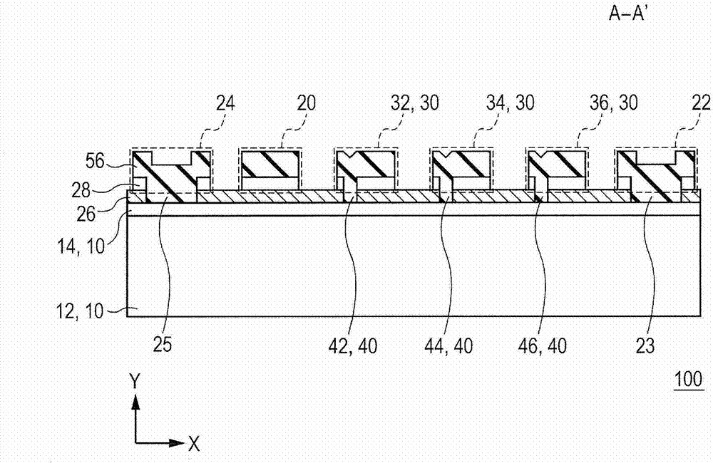
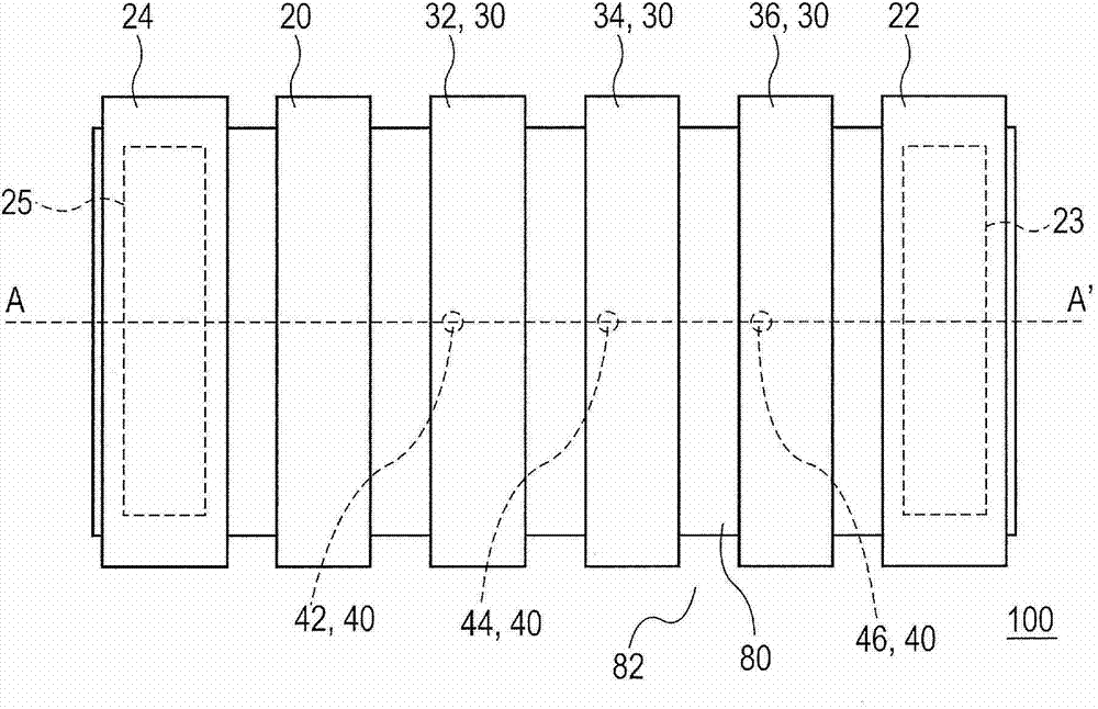
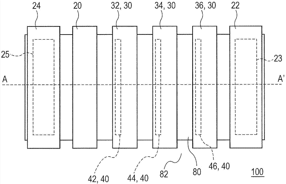
[0035] figure 1 is a cross-sectional view of the semiconductor device 100 according to the first embodiment of the present invention. The semiconductor device 100 includes a semiconductor substrate 10 , a gate electrode 20 , a source electrode 24 , a drain electrode 22 , at least one field plate electrode 30 and at least one field plate contact 40 . The semiconductor device 100 in this embodiment includes, for example, a high electron mobility transistor (HEMT).

[0036]The gate electrode 20 is arranged over the semiconductor substrate 10 . The source electrode 24 is arranged above the semiconductor substrate 10 . The source electrode 24 is spaced apart from the gate electrode 20 . In plan view, the drain electrode 22 is posi...


PUM


Abstract

The invention provides a semiconductor device and a method of manufacturing the same. The semiconductor device which provides compactness and enhanced drain withstand voltage. The semiconductor device includes: a gate electrode; a source electrode spaced from the gate electrode; a drain electrode located opposite to the source electrode with respect to the gate electrode in a plan view and spaced from the gate electrode; at least one field plate electrode located between the gate and drain electrodes in a plan view, provided over the semiconductor substrate through an insulating film and spaced from the gate electrode, source electrode and drain electrode; and at least one field plate contact provided in the insulating film, coupling the field plate electrode to the semiconductor substrate. The field plate electrode extends from the field plate contact at least either toward the source electrode or toward the drain electrode in a plan view.

Description

[0001] Cross references to related patent applications [0002] The disclosure of Japanese Patent Application No. 2011-196809 filed on Sep. 9, 2001 including specification, drawings and abstract is incorporated herein by reference in its entirety. technical field [0003] The present invention relates to semiconductor devices and methods of manufacturing semiconductor devices. Background technique [0004] In the field of semiconductor elements such as horizontal power MISFETs, it is necessary to increase the drain withstand voltage. The drain withstand voltage is evaluated based on whether a characteristic change or a breakdown phenomenon occurs in a semiconductor element when a rated voltage is continuously applied to the drain electrode with the gate voltage turned off. A characteristic change or a breakdown phenomenon occurring in a semiconductor element when a voltage is applied to a drain electrode is caused by electric field concentration in the semiconductor element...

Claims


Application Information

Patent Timeline
Patent Type & Authority Applications(China)
IPC IPC(8): H01L29/40H01L29/778H01L21/28H01L21/335
CPCH01L29/66659H01L29/7787H01L29/78H01L29/2003H01L29/402H01L29/404H01L29/66462H01L29/42316H01L29/7835H01L21/26546H01L29/0847H01L29/41758
Inventor 田中圣康
Owner RENESAS ELECTRONICS CORP
Why Eureka
Try Eureka