Semiconductor device and method for manufacturing semiconductor device

a semiconductor and semiconductor technology, applied in semiconductor devices, diodes, electrical equipment, etc., can solve problems such as breakdown voltage failure, leakage current increase, breakdown voltage failure, etc., to suppress the concentration of electric field and reduce the area of protective diodes

Active Publication Date: 2015-02-19
FUJI ELECTRIC CO LTD
View PDF1 Cites 10 Cited by
  • Summary
  • Abstract
  • Description
  • Claims
  • Application Information

AI Technical Summary

Benefits of technology

[0035]According to the semiconductor device and the method for manufacturing the semiconductor device according to the invention, the spreading of a depletion layer in a protective diode is suppressed and it is possible to reduce the area of the protective diode. In addition, according to the semiconductor device and the method for manufacturing the semiconductor device according to the invention, a pn junction surface between a p+ layer with high impurity concentration and an n− layer with low impurity concentration which form the protective diode is flattened (substantially perpendicular to a main surface of a substrate). Therefore, it is possible to suppress the concentration of the electric field on the pn junction surface.

Problems solved by technology

Therefore, a leakage current increases and a breakdown voltage failure occurs.
When the clamping voltage is frequently applied to the protective diode 105, the electric field is concentrated on the portion (pn junction surface 89) and the leakage current increases, which results in a breakdown voltage failure.

Method used


Image

  • Semiconductor device and method for manufacturing semiconductor device
  • Semiconductor device and method for manufacturing semiconductor device
  • Semiconductor device and method for manufacturing semiconductor device

Examples


first embodiment

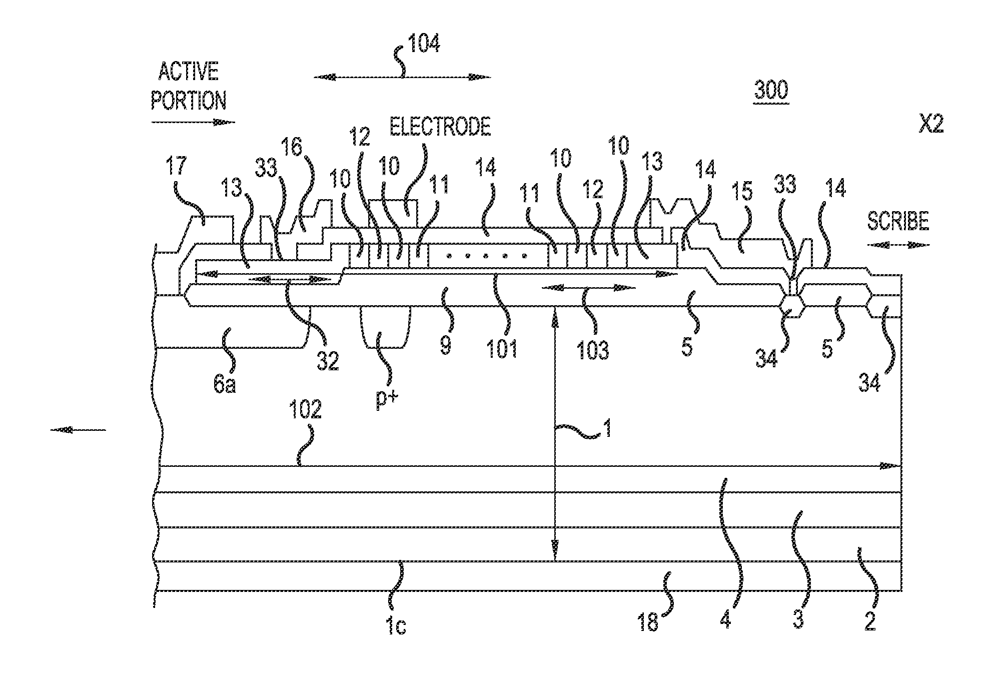
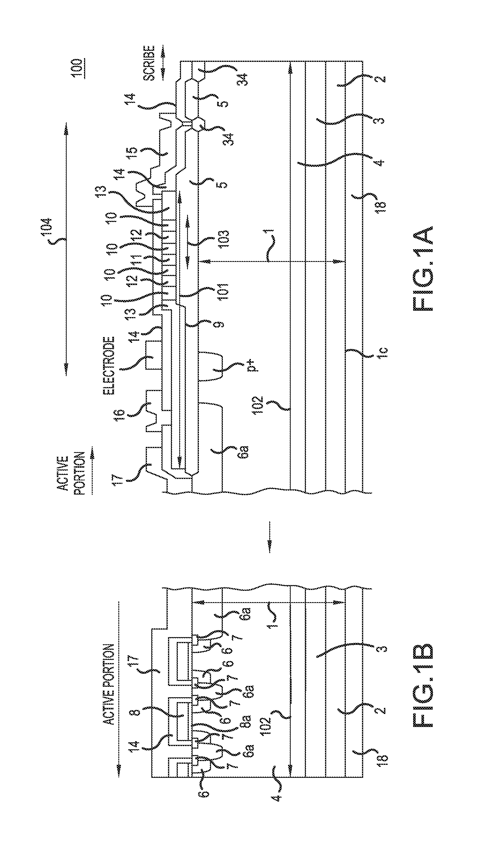
[0049]The structure of a semiconductor device forming an ignition IC of an internal-combustion engine ignition device will be described as an example of the structure of a semiconductor device according to a first embodiment of the invention. Since the circuit structure of the internal-combustion engine ignition device is the same as that of the internal-combustion engine ignition device 700 illustrated in FIG. 5, the description thereof will not be repeated. FIG. 1A is a cross-sectional view illustrating a main portion of the semiconductor device 100 in which a protective diode 101 is formed. FIG. 1B is a cross-sectional view illustrating a main portion in the vicinity of an active portion of the IGBT 102, which is connected to FIG. 1A. As illustrated in FIGS. 1A and 1B, the semiconductor device 100 according to the first embodiment has a structure in which an insulated gate bipolar transistor (IGBT) 102, which is a power semiconductor element, and the protective diode 101, which i...

second embodiment

[0064]Next, a method for manufacturing the protective diode of the semiconductor device according to the first embodiment illustrated in FIGS. 1A and 1B will be described as an example of a method for manufacturing a semiconductor device according to a second embodiment of the invention. FIGS. 4A, 4B, and 4C are diagrams illustrating the main manufacturing processes of the method for manufacturing the semiconductor device according to the second embodiment. Specifically, the manufacturing processes illustrated in FIGS. 4A, 4B, and 4C are manufacturing processes for the protective diode 101 illustrated in FIGS. 1A and 1B.

[0065]First, in FIG. 4A, an epitaxial substrate la obtained by epitaxially growing an n+ layer 3a (which will be the n buffer layer 3) and an n− layer 4a (which will be the n drift layer 4) in this order on the front surface of a thick p-type semiconductor base 2a (which will be the p collector layer 2) whose rear surface has not been ground is prepared. The sum of t...

third embodiment

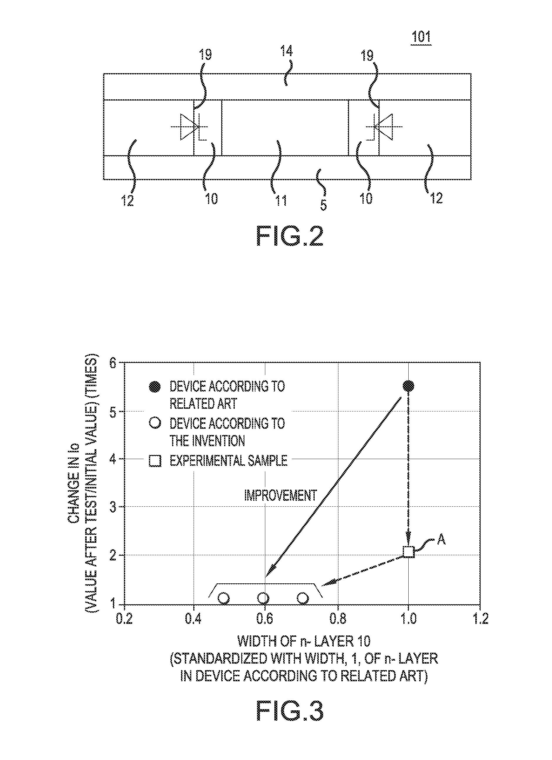
[0077]Next, the structure of a semiconductor device according to a third embodiment of the invention will be described. FIG. 9 is a plan view illustrating a main portion of a semiconductor device 200 according to the third embodiment of the invention. The semiconductor device 200 according to the third embodiment differs from the semiconductor device according to the first embodiment in that, in a protective diode 105 which is made of a polysilicon layer 9, high-resistance regions 20 are formed at both ends of a basic structure 103 in a direction perpendicular to the direction in which n+ / n− / p+ / n− layers are arranged in a line.

[0078]The high-resistance region 20 is formed in a substantially linear shape which extends from an n+ contact layer 13 which is provided on the inner circumferential side of the protective diode 105 to an n+ contact layer 13 which is provided on the outer circumferential side in the direction in which the layers of the protective diode 105 are arranged in a l...


PUM


Abstract

A protective diode has a basic structure including an n+ layer, an n layer, a p+ layer, and an n layer in this order. A p-type layer forming the protective diode is the p+ layer with high impurity concentration. Therefore, the spreading of a depletion layer is suppressed and it is possible to reduce the area of the protective diode. In addition, phosphorus ions with a large diffusion coefficient are implanted to form the n layer with low impurity concentration in the polysilicon layer forming the protective diode. A heat treatment is performed at a temperature of 1000° C. or higher to diffuse the phosphorus ions implanted into the polysilicon layer. Therefore, the impurity profile of the n layer in the depth direction can be uniformized in the depth direction.

Description

CROSS-REFERENCE TO RELATED APPLICATIONS[0001]This application is a continuation of International Application No. PCT / JP2013 / 080301, filed on Nov. 8, 2013, and is based on and claims priority to Japanese Patent Application No. 2012-246017, filed on Nov. 8, 2012 and Japanese Patent Application No. 2013-213270, filed on Oct. 11, 2013. The disclosure of the Japanese priority applications and the PCT application in their entirety, including the drawings, claims, and the specification thereof, are incorporated herein by reference.BACKGROUND[0002]1. Field of the Invention[0003]Embodiments of the present invention relate to a semiconductor device and a method for manufacturing a semiconductor device.[0004]2. Discussion of the Background[0005]An internal-combustion engine ignition device has been known which generates a high voltage from a low voltage and ignites a fuel-air mixture at a predetermined timing. FIG. 5 is a circuit diagram illustrating the structure of an internal-combustion eng...

Claims


Application Information

Patent Timeline
Patent Type & Authority Applications(United States)
IPC IPC(8): H01L29/78H01L29/06H01L21/265H01L29/66H01L29/40H01L21/02H01L29/866H01L29/739
CPCH01L29/7808H01L29/866H01L29/7811H01L29/0619H01L29/7395H01L21/26513H01L29/66712H01L29/402H01L21/02532H01L21/02595H01L29/66106H01L29/0692H01L29/0696H01L29/66121H01L29/861
Inventor NAITO, TATSUYA
Owner FUJI ELECTRIC CO LTD
Why Eureka
Try Eureka