Insulated gate semiconductor device, protection circuit and their manufacturing method

A technology of insulating gate type and manufacturing method, which is used in semiconductor/solid-state device manufacturing, emergency protection circuit devices, emergency protection circuit devices for limiting overcurrent/overvoltage, etc., can solve problems such as limitations, and achieve high sealing performance, reduce on-resistance, and ensure hermeticity

Inactive Publication Date: 2006-12-27
SANYO ELECTRIC CO LTD
View PDF1 Cites 9 Cited by
  • Summary
  • Abstract
  • Description
  • Claims
  • Application Information

AI Technical Summary

Problems solved by technology

However, in the above protection circuit in which two MOSFETs Q1 and Q2 are connected in series, there is a limit to this requirement.

Method used


Image

  • Insulated gate semiconductor device, protection circuit and their manufacturing method
  • Insulated gate semiconductor device, protection circuit and their manufacturing method
  • Insulated gate semiconductor device, protection circuit and their manufacturing method

Examples


Embodiment Construction

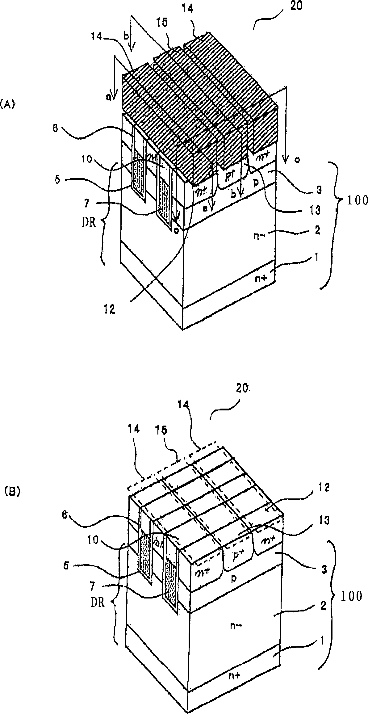
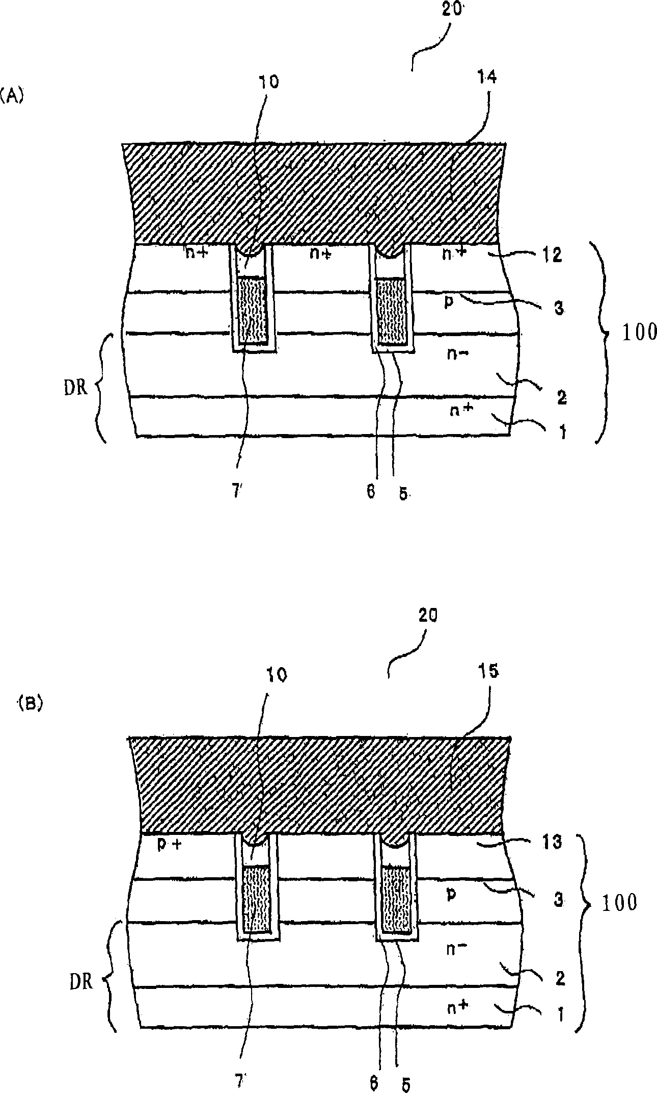
[0087] refer to Figure 1 to Figure 15 , the embodiment of the present invention will be described by taking a MOSFET with an n-channel layer trench structure as an example.

[0088] First, refer to Figure 1 to Figure 11 The first embodiment will be described. figure 1 It is a perspective view showing a MOSFET. figure 1 (A) is a figure in which the first and second electrode layers are arranged, figure 1 (B) is a diagram showing a region where the first and second electrode layers are arranged by dotted lines. in addition, figure 2 is a cross-sectional view, figure 2 (A) is figure 1 (A) a-a line profile, figure 2 (B) is figure 1 (A) The b-b line profile.

[0089] MOSFET20 consists of semiconductor substrate 1, semiconductor layer 2, channel layer 3, trench 5, gate insulating film 6, gate electrode 7, source region 12, body region 13, interlayer insulating film 10, first electrode layer 14. The second electrode layer 15 and the drain electrode 16 are formed. ...


PUM


Abstract

A first electrode layer (14), which comes into contact with a source region (12), and a second electrode layer (15), which comes into contact with a body (back gate) region (13), are provided. The first and second electrode layers (14, 15) are insulated from each other and are extended in a direction different from an extending direction of a trench (5). It is possible to individually apply potentials to the first and second electrode layers (14, 15), and to perform control for preventing a reverse current caused by a parasitic diode. Therefore, a bidirectional switching element can be realized by use of one MOSFET.

Description

technical field [0001] The present invention relates to an insulated gate semiconductor device, a method for manufacturing the same, and a protection circuit, that is, an insulated gate semiconductor device capable of performing bidirectional switching operations with one chip by separating the back gate, and a method for manufacturing the same. Background technique [0002] Figure 29 In , an n-channel MOSFET is shown as an example of a conventional semiconductor device. Figure 29 (A) is a floor plan, Figure 29 (B) is Figure 29 (A) The f-f line profile. in addition, Figure 29 In (A), the interlayer insulating film is omitted, and the source electrode is indicated by a dotted line. [0003] like Figure 29 (A), grooves 44 are formed in stripes on the surface of the substrate, and source regions 48 and body regions 49 are arranged adjacent to the grooves 44 . The trench 44, the source region 48, and the body region 49 extend in the same direction. [0004] like Figure ...

Claims


Application Information

Patent Timeline
Patent Type & Authority Applications(China)
IPC IPC(8): H01L29/78H01L21/336H01L27/02H02H9/00
CPCH01L29/66734H01L29/086H01L29/0696H01L29/7813H02J7/0029
Inventor 石田裕康万代忠男牛田敦也斋藤洋明
Owner SANYO ELECTRIC CO LTD
Why Eureka
Try Eureka