Semiconductor structure suitable for charge coupled device and manufacturing method of semiconductor structure

A technology of charge-coupled devices and semiconductors, applied in semiconductor/solid-state device manufacturing, semiconductor devices, electrical components, etc., can solve problems such as increased difficulty, achieve low manufacturing difficulty, and be conducive to yield and manufacturing cost control and compatibility Good results

Inactive Publication Date: 2016-06-15
WUXI NCE POWER
View PDF3 Cites 10 Cited by
  • Summary
  • Abstract
  • Description
  • Claims
  • Application Information

AI Technical Summary

Problems solved by technology

Therefore, the terminal design of charge-coupled devices is more difficult than that of general power devices.

Method used


Image

  • Semiconductor structure suitable for charge coupled device and manufacturing method of semiconductor structure
  • Semiconductor structure suitable for charge coupled device and manufacturing method of semiconductor structure
  • Semiconductor structure suitable for charge coupled device and manufacturing method of semiconductor structure

Examples


Embodiment Construction

[0048] The present invention will be further described below in conjunction with specific drawings and embodiments.

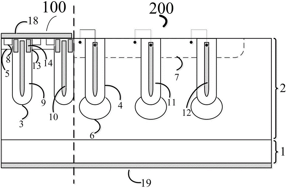
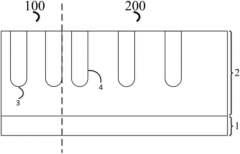
[0049] Such as figure 1 and Figure 12 Shown: In order to effectively improve the high-voltage resistance characteristics of the device, reduce the cost, and improve the scope of application, taking the semiconductor device of N-type MOSFET as an example, the present invention includes active components located on the semiconductor substrate on the top view plane of the semiconductor device. Area 100 and terminal protection area 200, the active area 100 is located in the central area of ​​the semiconductor substrate, the terminal protection area 200 is located at the outer circle of the active area 100 and surrounds the active area 100; in the cross section of the semiconductor device Above, the semiconductor substrate has two corresponding main surfaces, the two main surfaces include a first main surface and a second main surface corresponding to the first ma...


PUM


Abstract

The present invention relates to a semiconductor structure suitable for a charge-coupled device and a manufacturing method thereof. On the cross section of the semiconductor device, a second well region of a second conductivity type is provided in a first conductivity type drift region of a terminal protection region, The second well region of the second conductivity type is located in the upper part of the drift region of the first conductivity type, and a plurality of terminal trenches are arranged in the terminal protection zone, and the terminal trenches are located in the second well region of the second conductivity type, and the depth extends to into the drift region of the first conductivity type under the second well region of the second conductivity type; the termination dielectric body and the terminal conductor are filled in the termination trench, and the termination conductor is the same as the adjacent active region outside the termination trench The second conductivity type second well region on the side is electrically connected. The invention has a compact structure, can effectively improve the high-voltage resistance characteristic of the device, is compatible with the existing technology, reduces the cost, has wide application range, and is safe and reliable.

Description

technical field [0001] The invention relates to a semiconductor device and a manufacturing method thereof, in particular to a semiconductor structure suitable for a charge-coupled device and a manufacturing method thereof, belonging to the technical field of semiconductor devices. Background technique [0002] Regulatory agencies and end customers are increasingly demanding DC-DC power supply efficiency, and new designs require lower on-resistance without compromising unclamped inductive switching (UIS) capability or increasing switching losses. [0003] DC-DC designers are always challenged to improve efficiency and power density. On-resistance (Rds-on) and gate charge (Qg) are two key parameters of power semiconductors. Generally, one always decreases while the other increases. Therefore, power MOSFET designers must consider the trade-off between the two, and the continuous advancement of power MOSFET technology helps them alleviate this contradiction. The charge-coupled ...

Claims


Application Information

Patent Timeline
Patent Type & Authority Applications(China)
IPC IPC(8): H01L29/06H01L29/78H01L21/336
CPCH01L29/0611H01L29/66477H01L29/78
Inventor 朱袁正叶鹏刘晶晶
Owner WUXI NCE POWER
Why Eureka
Try Eureka