Semiconductor device manufacturing method and semiconductor device

Active Publication Date: 2011-02-24
SHARP KK
View PDF9 Cites 10 Cited by
  • Summary
  • Abstract
  • Description
  • Claims
  • Application Information

AI Technical Summary

Benefits of technology

[0043]Therefore, in accordance with the present invention, the aforementioned problems (1) to (3) associated with the conventional technique are all solved, and a transistor having an excellent characteristic, which is superior in terms of dielectric strength voltage and whose transfer characteristics is free of kink can be mounted on the active region having been subjected to the element isolation by the STI. Thus, it becomes possible to manufacture a substrate on which

Problems solved by technology

This results in the presence of kink in the transfer characteristic of the transistor formed on the active region.
With the liquid crystal driver, such presence of kink in the transfer characteristic of the transistor causes incorrect gradation expression of a displayed image, which eventually leads to a poor image display performance of the liquid crystal display or the liquid crystal television set.
Further, when the kink is significant, the leak current when the transistor is turned off becomes large, posing problems such as an increase in power consu

Method used


Image

  • Semiconductor device manufacturing method and semiconductor device
  • Semiconductor device manufacturing method and semiconductor device
  • Semiconductor device manufacturing method and semiconductor device

Examples


first embodiment

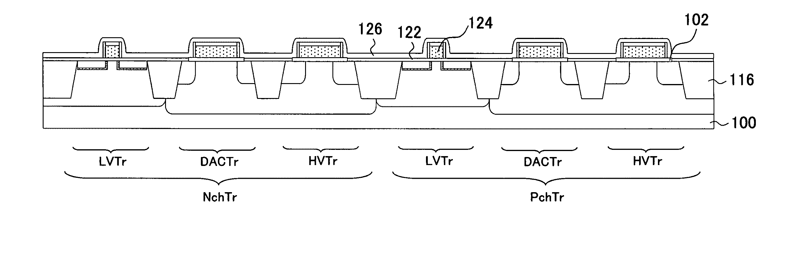
[0060]In the following, a description will be given in detail of a semiconductor device manufacturing method according to an embodiment of the present invention (hereinafter, referred to as “the method of present invention” as appropriate). FIGS. 5A to 9C are cross-sectional views each schematically showing a workpiece in a step in the semiconductor device manufacturing method of the present invention. Note that, in the present embodiment, while the description will be given of an exemplary case in which the present invention is employed in manufacturing liquid crystal driver ICs used for controlling the display operation of liquid crystal displays, liquid crystal television sets and the like, the present invention is not limited thereto. In FIGS. 5A to 9C, the reference character NchTr denotes a portion where an N channel transistor is formed, and the reference character PchTr denotes a portion where a P channel transistor is formed. The reference character LVTr denotes each active...

second embodiment

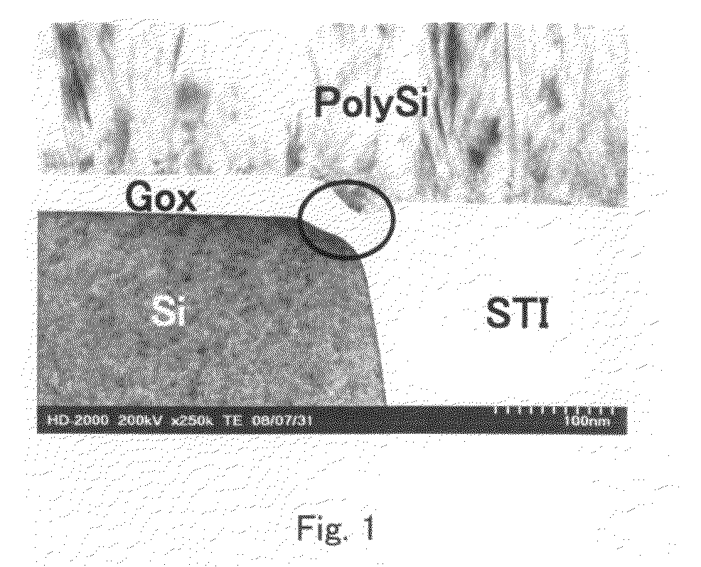
[0080]An SEM cross-sectional picture of an STI formed according to the method of the present invention is shown in FIG. 10 as an example. As shown in FIG. 10, it can be seen that, by applying the method of the present invention, a reduction in thickness of the gate oxide film at the STI corner portion is suppressed, and that the gate oxide film (Gox) whose top surface is flat across the active regions is obtained. Further, owing to the fact that the gate oxide film is formed before the STI is formed, the top surface of the gate oxide film is positioned at a position lower than the top surface of the element isolation film of the STI. On the other hand, in the peripheral portion of each active region, the bottom surface of the gate oxide film has a rounded shape whose depthwise position is inclined downward as approaching the boundary with the STI.

[0081]FIG. 11 is an SEM cross-sectional picture of the semiconductor substrate, after the trench is formed and the field insulating film 1...


PUM


Abstract

A formation method of an element isolation film according to which a high-voltage transistor with an excellent characteristic can be formed is provided. On a substrate, a gate oxide film is previously formed. A CMP stopper film is formed thereon, and thereafter, a gate oxide film and a CMP stopper film are etched. The semiconductor substrate is etched to form a trench. Further, before the trench is filled with a field insulating film, an liner insulating film is formed at a trench interior wall, and a concave portion at the side surface of the gate oxide film under the CMP stopper film is filled with the liner insulating film. In this manner, formation of void in the element isolation film laterally positioned with respect to the gate oxide film can be prevented.

Description

CROSS REFERENCE TO RELATED APPLICATION[0001]This Nonprovisional application claims priority under 35 U.S.C. §119(a) on Patent Application No. 2009-190456 filed in Japan on 19 Aug., 2009 the entire contents of which are hereby incorporated by reference.BACKGROUND OF THE INVENTION[0002]1. Field of the Invention[0003]The present invention relates to a semiconductor device manufacturing method and a semiconductor device. In particular, the present invention relates to a formation method of an element isolation region for electrically isolating semiconductor elements from each other that are formed on a semiconductor substrate.[0004]2. Description of the Related Art[0005]As a method for electrically isolating semiconductor elements from each other, what is frequently used is a method including a step of forming a trench between active regions where semiconductor elements are to be formed on a substrate, and a step of filling the trench with an insulating material, so as to form an STI (S...

Claims


Application Information

Patent Timeline
IPC IPC(8): H01L29/772H01L21/762
CPCH01L29/78H01L21/76224
Inventor TAJIRI, MASAYUKIHASHIMOTO, TAKAYOSHIYONEMOTO, HISASHIHARAZONO, TOYOHIRO
Owner SHARP KK
Why Eureka
Try Eureka