Schottky barrier diode

a barrier diode and diode technology, applied in the field of schottky barrier diodes, can solve the problems of reverse pressure resistance reduction, achieve the effects of reducing the forward voltage reducing the leakage current of the schottky barrier diode, and increasing the specific resistance of the n-type epitaxial layer

Active Publication Date: 2015-08-13
ROHM CO LTD
View PDF1 Cites 6 Cited by
  • Summary
  • Abstract
  • Description
  • Claims
  • Application Information

AI Technical Summary

Benefits of technology

[0006]One of important properties of the Schottky barrier diode is that a leakage current is small at a time of applying the reverse voltage. Further, another important property is that a forward voltage for bringing into a conduction state is low. In order to decrease the leakage current of the Schottky barrier diode, it is preferable to increase a specific resistance of the n-type epitaxial layer. On the other hand, in order to decrease the forward voltage of the Schottky barrier diode

Problems solved by technology

However, this measure causes decrease of a reverse pressure resistance (hereinaft

Method used


Image

  • Schottky barrier diode
  • Schottky barrier diode
  • Schottky barrier diode

Examples


first embodiment

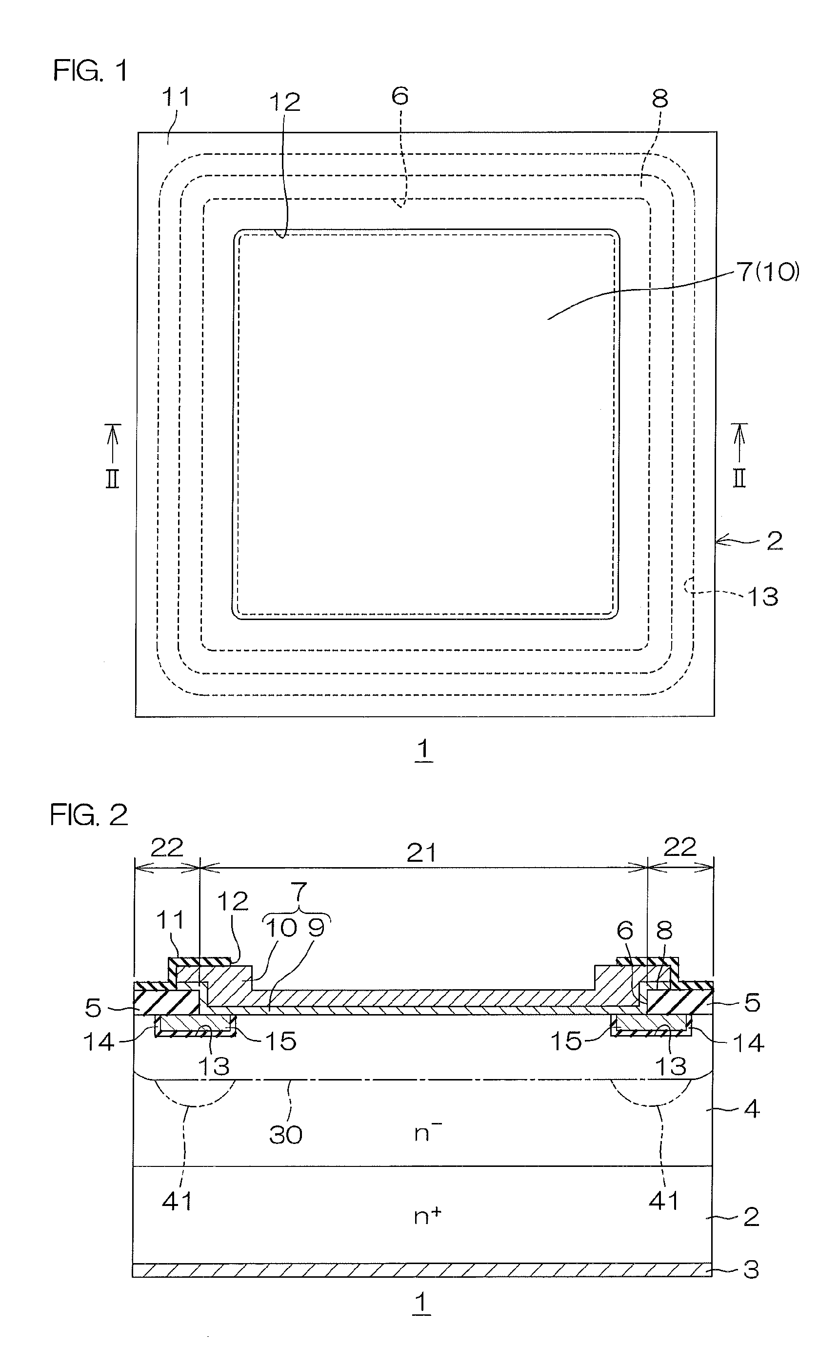
[0041]FIG. 1 is a plan view showing a Schottky barrier diode according to the present invention.

[0042]FIG. 2 is a sectional view along a line II-II in FIG. 1.

[0043]The Schottky barrier diode 1 is formed in a quadrangular chip shape in plan view, as shown in FIG. 1, for example. Each length of four sides of the Schottky barrier diode 1 in plan view is several millimeters, for example.

[0044]The Schottky barrier diode 1 comprises a semiconductor substrate 2 formed of n+-type (whose n-type impurity concentration is 1×10¹⁸ to 1×1021 cm−3, for example) silicone (Si) . A cathode electrode 3 is formed on a rear surface of the semiconductor substrate 2 to cover an entire area thereof. The cathode electrode 3 is formed of a metal (Au, nickel (Ni) silicide and cobalt silicide, for example) which is brought into ohmic contact with an n-type silicone.

[0045]An epitaxial layer 4 formed of an n−-type (whose n-type impurity concentration is 1×10¹⁵ to 1×1017 cm−3, for example) silicone with a concent...

second embodiment

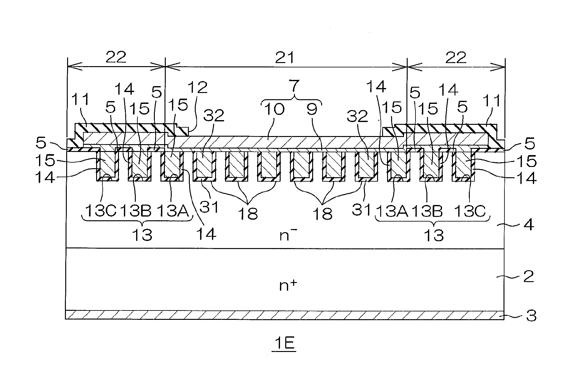
[0077]FIG. 7 is a schematic plan view showing a Schottky barrier diode according to the present invention. FIG. 8 is a sectional view along a line VIII-VIII in FIG. 7. Portions in FIGS. 7 and 8 corresponding to the respective portions shown in above-described FIGS. 1 and 2 have the same reference symbols.

[0078]A Schottky barrier diode 1A of the second embodiment is different from the Schottky barrier diode 1 of the first embodiment in that a plurality of inside trenches 18 are formed in a surface layer portion of an epitaxial layer 4 on a region in an opening 6 of a field insulating film 5, and in that a Schottky metal 9 is formed to contact a surface of the epitaxial layer 4 including inner wall surfaces of each inside trench 18. That is, while the Schottky barrier diode 1 of the first embodiment is a planar Schottky barrier diode, the Schottky barrier diode 1A of the second embodiment is a trench junction Schottky barrier diode.

[0079]Points different from the first embodiment are ...

third embodiment

[0096]FIG. 10 is a plan view showing a Schottky barrier diode according to the present invention. FIG. 11 is a sectional view along a line XI-XI in FIG. 10. Portions in FIGS. 10 and 11 corresponding to the respective portions shown in above-described FIGS. 1 and 2 have the same reference symbols.

[0097]A Schottky barrier diode 1B of the third embodiment is different from the Schottky barrier diode 1 of the first embodiment in that a field insulating film is not formed on a peripheral portion of an epitaxial layer 4.

[0098]Points different from the first embodiment are described more specifically below. In this Schottky barrier diode 1B, an anode electrode 7 which is quadrangular in plan view is formed on a center region except a peripheral portion of a surface of the epitaxial layer 4. The anode electrode 7 has a multi-layer structure (two-layer structure in this embodiment) of a Schottky metal 9 being in Schottky junction with the epitaxial layer 4 and an electrode metal 10 laminated...


PUM


Abstract

A Schottky metal 9 is in Schottky-contact with a center portion of a surface of an epitaxial layer 4. A peripheral trench 13 is formed by digging from the surface of the epitaxial layer 4 on a boundary portion between an active region 21 where the Schottky metal 9 is in Schottky-contact with the surface of the epitaxial layer 4 and a peripheral region 22 outside of the active region in a surface layer portion of the epitaxial layer 4. An insulating film 14 is formed on an entire area of inner wall surfaces of the peripheral trench 13. There is provided with a conductor 15 which is connected to the Schottky metal 9 and is opposed to the entire area of the inner wall surfaces of the peripheral trench 13 via the insulating film 14 in the peripheral trench 13.

Description

BACKGROUND OF THE INVENTION[0001]1. Field of the Invention[0002]The present invention relates to a Schottky barrier diode.[0003]2. Description of the Related Art[0004]A Schottky barrier diode includes an n-type semiconductor substrate, an n-type epitaxial layer formed on the n-type semiconductor substrate, and a Schottky metal which is in Schottky-contact with a surface of the n-type epitaxial layer. The surface of the n-type epitaxial layer includes an active region where the Schottky metal is in Schottky-contact with the surface of the n-type epitaxial layer, and a peripheral region outside thereof. When a reverse voltage is applied to the Schottky barrier diode, an electric field is concentrated on a boundary portion between the active region and the peripheral region. Therefore, in order to alleviate concentration of the electric field, a configuration is known where a p-type region (p-type guard ring) across the active region and the peripheral region is formed on the boundary ...

Claims


Application Information

Patent Timeline
IPC IPC(8): H01L29/872H01L29/47
CPCH01L29/47H01L29/8725H01L29/407H01L29/66143H01L29/872
Inventor SUGIURA, HIROTO
Owner ROHM CO LTD
Why Eureka
Try Eureka