Sputtering target material and sputtering device

A sputtering target and sputtering device technology, which is applied in sputtering coating, metal material coating process, ion implantation coating, etc., can solve the problems of uniform distribution of plasma 120, low target utilization rate, and target Eliminate material consumption and other issues, achieve the effect of improving film quality uniformity, increasing service life, and improving product yield

Active Publication Date: 2013-04-03
BOE TECH GRP CO LTD +1
View PDF5 Cites 6 Cited by
  • Summary
  • Abstract
  • Description
  • Claims
  • Application Information

AI Technical Summary

Problems solved by technology

When such a target is used for coating, the distribution of the lateral plasma 120 generated in the chamber of the sputtering equipment is as follows: figure 2 As shown, the plasma 120 is in an inverted U-shaped distribution with concentrated distribution in the middle of the width direction of the strip block 110 and less edge distribution, and the uniformity of the distribution of the plasma 120 is relatively poor.
In this way, after a period of use, the target material in the middle of the strip-shaped block 110 intensively impacted by the plasma 120 is seriously consumed, while the target material in the edge position of the strip-shaped block is less consumed, forming a pattern such as image 3 The waste area shown makes the utilization rate of the target material low and causes serious waste; similarly, the labor cost required for frequent material replacement cannot be ignored

Method used


Image

  • Sputtering target material and sputtering device
  • Sputtering target material and sputtering device
  • Sputtering target material and sputtering device

Examples


Embodiment Construction

[0019] The present invention will be described in detail below in conjunction with the accompanying drawings and embodiments.

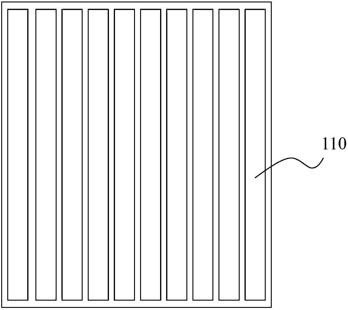
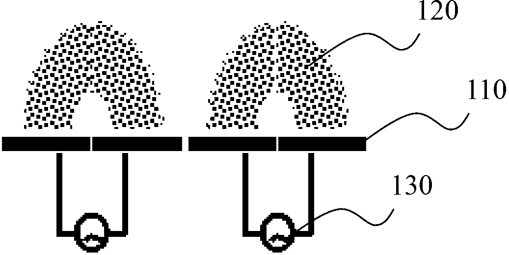
[0020] Figure 4 Shown is a schematic structural view of a sputtering target described in this embodiment, the sputtering target includes a plurality of first blocks A and a plurality of second blocks B, and the plurality of first blocks A and the second block B are distributed in multiple rows and columns, wherein the first block A and the second block B in each row are staggered, and in each column the first block A and the second block Block B is also staggered.

[0021] The first sub-block A and the second sub-block B of the above-mentioned row and column staggered distribution are respectively connected to two electrodes with opposite polarities of the AC power supply when in use. When the two electrodes of the AC power supply are switched between forward and reverse polarity, The first block A and the second block B also switch the anode and t...


PUM


Abstract

The invention discloses a sputtering target material, comprising a plurality of first sub-blocks and a plurality of second sub-blocks, wherein the plurality of first sub-blocks and the plurality of second sub-blocks are distributed in a plurality of rows and columns; the first sub-blocks and the second sub-blocks in each row are distributed in a staggered manner; and the first sub-blocks and the second sub-blocks in each column are also distributed in the staggered manner. A sputtering device comprising the sputtering target material is also disclosed by the invention; the sputtering device comprises an alternating current power supply; the alternating current power supply comprises a first electrode and a second electrode, of which the polarities are opposite; each first sub-block of the sputtering target material is correspondingly connected with the first electrode of the alternating current power supply; and each second sub-block of the sputtering target material is correspondingly connected to the second electrode of the alternating current power supply. The sputtering target material is designed into blocks, so that the target material is fully utilized, and a product membrane has good uniformity.

Description

technical field [0001] The invention relates to the technical field of sputtering processing, in particular to a sputtering target and a sputtering device. Background technique [0002] In the TFT-LCD array manufacturing process, as the size of the glass substrate continues to increase, the current AC mode (AC mode) sputtering equipment has become the mainstream equipment for magnetron sputtering, and its advantages are less abnormal discharge and better film formation. Good uniformity. figure 1 Shown is a schematic diagram of the target material used in the TFT-LCD manufacturing process in the prior art. It can be seen that the entire target material is evenly divided into a plurality of strip-shaped blocks 110 parallel to each other. The AC voltage of the AC power supply 130 is connected between each strip block 110 , so that the anode and cathode can be freely switched between each strip block 110 . When such a target is used for coating, the distribution of the lateral...

Claims


Application Information

Patent Timeline
Patent Type & Authority Applications(China)
IPC IPC(8): C23C14/34
Inventor 王文龙段献学白明基
Owner BOE TECH GRP CO LTD
Why Eureka
Try Eureka