Flat multichip packaging piece with stamping frame with square groove and production method of flat multichip packaging piece

A technology of multi-chip packaging and square grooves, applied in semiconductor/solid-state device manufacturing, electrical components, electrical solid-state devices, etc., can solve problems such as performance degradation, product defects, failures, etc., to reduce the possibility of delamination, Improve product reliability and solve the effect of high cost

Inactive Publication Date: 2013-04-03
HUATIAN TECH XIAN
View PDF4 Cites 8 Cited by
  • Summary
  • Abstract
  • Description
  • Claims
  • Application Information

AI Technical Summary

Problems solved by technology

[0005]1. The combination of integrated circuit chip and carrier is not good. When affected by changes in the external environment, it will cause layered defects inside the product, resulting in performance degradation , or even fail;
[0006

Method used


Image

  • Flat multichip packaging piece with stamping frame with square groove and production method of flat multichip packaging piece
  • Flat multichip packaging piece with stamping frame with square groove and production method of flat multichip packaging piece

Examples


Example Embodiment

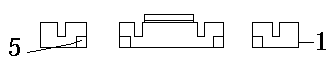
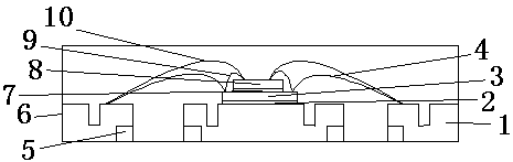
[0015] As shown in the figure, a flat multi-chip package with a stamping frame with a square groove is mainly composed of a lead frame 1, a square groove 5, a lower chip 3, an upper chip 8, a lower adhesive sheet 2, and an upper adhesive sheet. The glue 7, the lower bonding wire 4, the middle bonding wire 9, the upper bonding wire 10 and the plastic sealing body 6 are composed; the lead frame 1 is provided with a square groove 5, and the lead frame 1 is connected with The lower chip 3 is bonded, the lower chip 3 is bonded to the upper chip 8 through the upper adhesive sheet 7, the lower bonding wire 4 is connected to the lead frame 1 and the lower chip 3, and the middle bonding wire 9 is connected to the lower bonding wire. Sheet glue 2 and upper sheet glue 7, the upper bonding wire 10 connects the upper sheet glue 7 and the lead frame 1, the plastic package 6 surrounds the lead frame 1, the lower chip 3, the upper chip 8, and the lower sheet glue 2. The upper adhesive 7, the ...


PUM


Abstract

The invention discloses a flat multichip packaging piece with a stamping frame with a square groove and a production method of the flat multichip packaging piece. The packaging piece mainly comprises a lead frame, the square groove, a lower chip, an upper chip, a lower surface mount adhesive, an upper surface mount adhesive, a lower bonding wire, a middle bonding wire, an upper bonding wire and a plastic package body, the square groove is reserved on the lead frame which is adhered with the lower chip through the lower surface mount adhesive, the lower chip is adhered with the upper chip via the upper surface mount adhesive, the lower bonding wire is connected with the lead frame and the lower chip, the middle bonding frame is connected with the upper surface mount adhesive and the upper surface mount adhesive, the upper bonding wire is connected with the upper surface mount adhesive and the lead frame, the plastic package body surrounds the lead frame, the lower chip, the upper chip, the lower surface mount adhesive, the upper surface mount adhesive, the lower bonding wire, the middle bonding wire and the upper bonding wire and particularly fills the square groove, and the lead frame, the lower chip, the upper chip, the lower bonding wire, the middle bonding wire and the upper bonding wire form a power source and a signal channel of a circuit. The plastic package body is combined with the lead frame more firmly, and delamination-resisting effect is better.

Description

[0001] technical field [0002] The invention belongs to the technical field of integrated circuit packaging, in particular to a flat multi-chip package with a stamping frame with square grooves and a manufacturing method thereof. Background technique [0003] QFN (four-sided flat no-lead package) and DFN (dual flat no-lead package) packages have been developed in recent years with the emergence of communication and portable small digital electronic products (digital cameras, mobile phones, PCs, MP3) , Applicable to the packaging of small and medium-sized integrated circuits with high frequency, broadband, low noise, high thermal conductivity, small volume, high speed and other electrical requirements. We know that the QFN / DFN package effectively utilizes the package space of the lead pins, thereby greatly improving the package efficiency. However, at present, most semiconductor packaging manufacturers face some difficulties in the selection of frames in the manufacturing p...

Claims


Application Information

Patent Timeline
IPC IPC(8): H01L23/495H01L25/00H01L21/50
CPCH01L24/73H01L2224/32145H01L2224/32245H01L2224/48145H01L2224/48247H01L2224/73265
Inventor 郭小伟蒲鸿鸣崔梦刘卫东朱文辉
Owner HUATIAN TECH XIAN
Why Eureka
Try Eureka