LED packaging structure utilizing distant fluorescent powder layer and manufacturing method of LED packaging structure

A technology of LED packaging and phosphor layer, which is applied in the field of LED packaging structure and its manufacture, can solve the problems of disturbing chip light, uneven thickness, damage, etc., and achieve the effects of mass production, cost saving and simple technology

Active Publication Date: 2013-04-03
HKUST LED FPD TECH R&D CENT AT FOSHAN
View PDF5 Cites 9 Cited by
  • Summary
  • Abstract
  • Description
  • Claims
  • Application Information

AI Technical Summary

Problems solved by technology

This means that the light emitted from the chip touches the phosphor. This light output mode has two disadvantages: 1. Part of the light is directly reflected back to the chip by the phosphor, and this part of the light disturbs the light emitted by the chip.
2. The heat generated by the chip is directly transmitted to the phosphor layer, which accelerates the temperature rise of the phosphor, directly damages and reduces the life of the phosphor, and causes LED lamp reliability problems
[0007] Common defects of existing phosphor powder coating technology: First, the common bracket LED chip packaging is to pour excessive fluorescent glue into the reflective cup without control to achieve the effect of emitting white light
For factory mass production sales, fully conformal coating technology requires too large implementation cost
Another process is to slightly control the coating of the phosphor, and only coat the phosphor around the chip, but because there is no ideal process, the phosphor layer with uneven thickness and irregular shape is often obtained.

Method used


Image

  • LED packaging structure utilizing distant fluorescent powder layer and manufacturing method of LED packaging structure
  • LED packaging structure utilizing distant fluorescent powder layer and manufacturing method of LED packaging structure
  • LED packaging structure utilizing distant fluorescent powder layer and manufacturing method of LED packaging structure

Examples


Embodiment 1

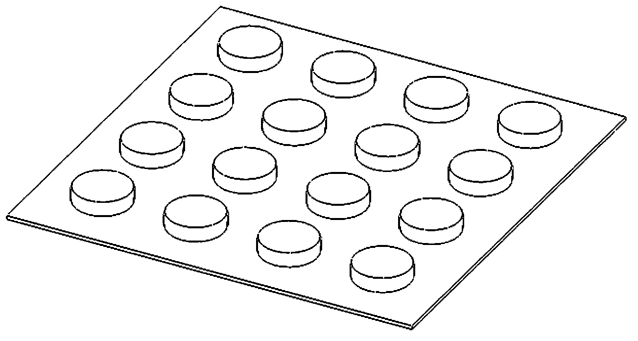
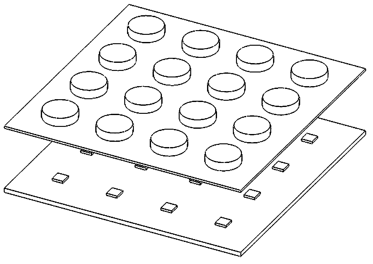
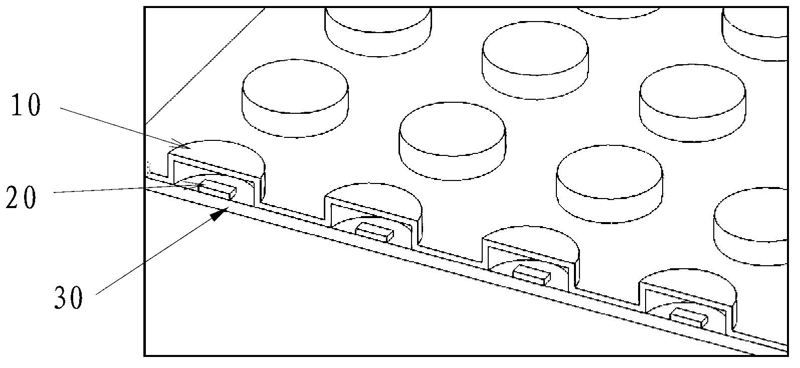
[0060] refer to Figure 1-3 , an LED packaging structure in this embodiment, comprising a substrate 30, an LED chip 20 and a phosphor layer 10, the LED chip 20 is fixed on the substrate 30, the phosphor layer 10 is a cover-like structure with a concave cavity, and the fluorescent The powder layer is bonded on the substrate, the phosphor layer and the substrate form a closed cavity, the LED chip is covered in a concave cavity, the volume of the concave cavity is larger than the volume of the LED chip, and the phosphor layer The space between the LED chip and the LED chip is a vacuum.

[0061] The shape of the concave cavity is cylindrical.

[0062] The preparation method of the above-mentioned fluorescent powder layer comprises the following steps: using a male mold and a female mold whose shapes cooperate with each other to prepare, the female mold is provided with at least one concave cavity, and the male mold is provided with a cavity that is compatible with the concave cav...

Embodiment 2

[0080] refer to Figure 7-9 In this embodiment, an LED packaging structure includes a substrate, an LED chip and a phosphor layer, the LED chip is fixed on the substrate, the phosphor layer is a cover-like structure with a concave cavity, and the phosphor layer is bonded to the substrate , the phosphor layer and the substrate form a closed cavity, the LED chip is covered in a concave cavity, the volume of the concave cavity is larger than the volume of the LED chip, and the gap between the phosphor layer and the LED chip The space between is vacuum.

[0081] The shape of the concave cavity is hemispherical.

[0082] The preparation method of the above-mentioned fluorescent powder layer comprises the following steps: using a male mold and a female mold whose shapes cooperate with each other to prepare, the female mold is provided with at least one concave cavity, and the male mold is provided with a cavity that is compatible with the concave cavity. The convex structure match...


PUM

PropertyMeasurementUnit
luminous efficiencyaaaaaaaaaa
thicknessaaaaaaaaaa

Abstract

The invention discloses an LED packaging structure utilizing a distant fluorescent powder layer and a manufacturing method of the LED packaging structure. The packaging structure uses the fluorescent powder layer of a concave cavity cover structure. A die for manufacturing the fluorescent powder layer is designed specifically. The fluorescent powder layer manufactured by the die is regular in structure and even in thickness. The fluorescent powder layer and a substrate forms a closed vacuum cavity for accommodating a chip on the substrate, and accordingly distant fluorescent powder coating is achieved. The manufacturing method is also applicable to fluorescent powder layer manufacturing in batch, repeated adhesive dispense for each chip in traditional batch fluorescent powder layer packaging process, and LED packaging efficiency is improved.

Description

technical field [0001] The invention relates to the technical field of LED packaging, in particular to the preparation of a fluorescent powder structure with uniform thickness, in particular to an LED packaging structure using a remote phosphor layer and a manufacturing method thereof. Background technique [0002] LED (Light Emitting Diode), a light-emitting diode, is a solid-state semiconductor device that can directly convert electrical energy into light energy. It changes the principle of incandescent lamp tungsten filament luminescence and energy-saving lamp three-based toner luminescence, and uses electric field luminescence. The characteristics of LED are very obvious, such as long life, high luminous efficiency, low radiation and low power consumption. The spectrum of white LEDs is almost entirely concentrated in the visible light band, and its luminous efficiency can exceed 150lm / W (2010). [0003] LED packaging refers to the packaging of light-emitting chips, whi...

Claims


Application Information

Patent Timeline
Patent Type & Authority Applications(China)
IPC IPC(8): H01L33/50H01L33/48
CPCF21K9/64F21K9/90F21Y2105/10F21Y2115/10H01L25/0753H01L33/505H01L33/507H01L2924/0002H01L2933/0041H01L2924/00
Inventor 刘惠华卢智铨张荣李世玮
Owner HKUST LED FPD TECH R&D CENT AT FOSHAN
Why Eureka
Try Eureka