Vcsel semiconductor devices with mode control

A conductor and active layer technology, applied in semiconductor lasers, laser parts, electrical components, etc., can solve problems such as high junction temperature, loss, and shortened optical life.

Inactive Publication Date: 2007-09-19
EMCORE INC
View PDF5 Cites 28 Cited by
  • Summary
  • Abstract
  • Description
  • Claims
  • Application Information

AI Technical Summary

Problems solved by technology

Correspondingly, low output power limits the length of any optical link using this design
[0021] 2. As detailed in this patent (eg Figures 3A, 3B, 7A, 7B, 8A, 8B...), in order to select a high-order single mode, a complex and precise pattern must be used in the fabrication of the laser
Smaller apertures reduce the number of allowable transverse modes, but there are a number of issues related to device reliability: First, device resistance is inversely proportional to the square of the aperture diameter
Smaller devices have higher junction temperatures and thus shorter wear-out lifetimes
Fifth, a smaller aperture requires a higher proportion of oxidized AlGaAs, which increases the mechanical strain in the laser
Second, the AEM die has additional losses due to scattering from the oxide aperture
The end result is a shortened optical lifetime and allows the optical mode to better track the drive current when modulating the laser

Method used


Image

  • Vcsel semiconductor devices with mode control
  • Vcsel semiconductor devices with mode control
  • Vcsel semiconductor devices with mode control

Examples


Embodiment Construction

[0051] Details of the invention, including exemplary aspects and embodiments thereof, are set forth below. Referring to the drawings and the following detailed description, like reference numerals are used to designate like or functionally similar elements and are intended to illustrate major features of example embodiments in an extremely simplified illustration. Moreover, the drawings are not intended to depict every feature of actual embodiments nor relative dimensions of the elements shown, nor are they drawn to scale.

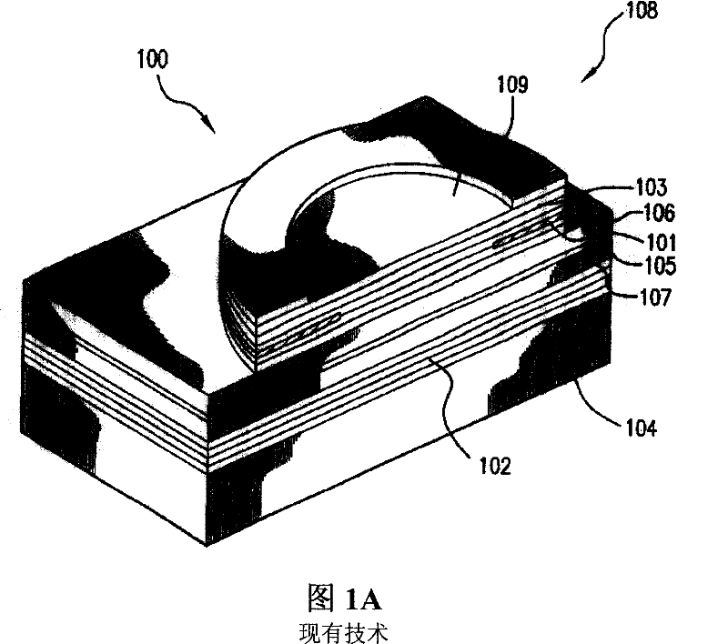
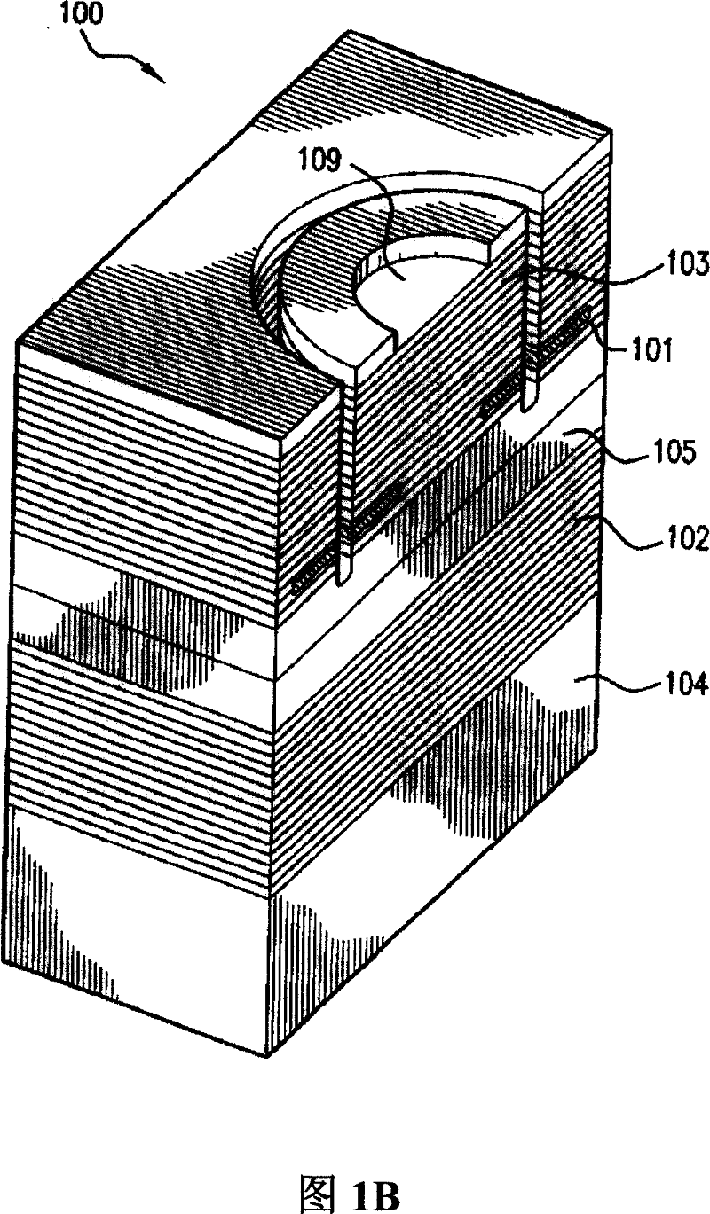
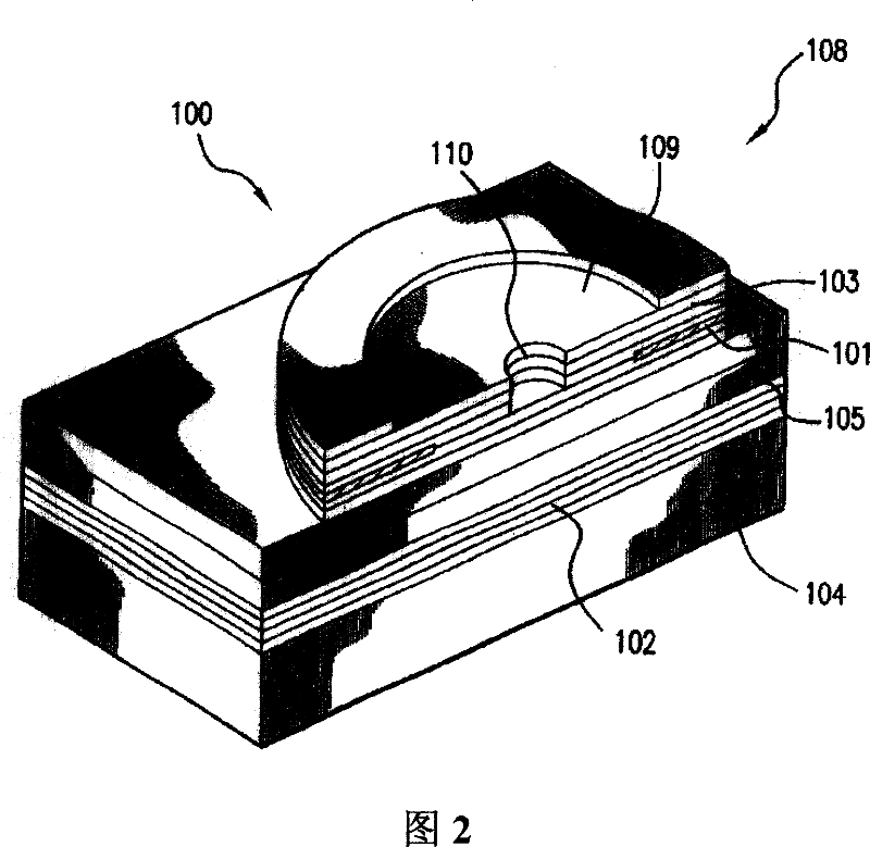
[0052] Referring to FIG. 1a, it shows a partial cross-sectional view of a semiconductor structure of an oxide-confined VCSEL known in the prior art. Specifically, the VCSEL 100 includes a laser cavity region 105 defined between a first semiconductor region 102 forming a first mirror stack and a second semiconductor region 103 forming a second mirror stack. between. Semiconductor regions 102 and 103 are disposed on a substrate 104 which may typically be p...


PUM


Abstract

A surface emitting laser having a substrate with top and bottom surfaces; a first stack of mirror layers of alternating indices of refraction located upon the top surface of the substrate; and active layer disposed over the first stack; a second stack of mirror layers of alternating indices of refraction disposed over the active layer and a recessed portion located centrally in the second stack extending through at least some of the second stack of mirror layers for improving the spectral width characteristic of the laser.

Description

technical field [0001] The present invention relates to vertical cavity surface emitting lasers (VCSELs), and more particularly to VCSELs with mode control formed by selective patterning of upper mirror or mesa structures. Background technique [0002] A typical VCSEL configuration includes an active region located between two mirrors placed one above the other on the surface of the substrate wafer. An insulating region between the mirrors forces current to flow through a small aperture, and the device emits laser light perpendicular to the wafer surface (ie, the "vertical" portion of the VCSEL). One type of VCSEL—specifically, the proton VCSEL in which the insulating region is formed by a proton implantation—dominated the early commercial history of VCSELs. In oxide-guided VCSELs, the insulating region is formed by partially oxidizing a thin, high-aluminum layer within the mirror structure. This same oxidation process can be applied to other semiconductor structures to pr...

Claims


Application Information

Patent Timeline
Patent Type & Authority Applications(China)
IPC IPC(8): H01S5/183H01S5/00
CPCH01S5/0422H01S5/18391H01S2301/166H01S2301/203H01S5/18327H01S5/18311
Inventor 道格·柯林斯李念宜
Owner EMCORE INC
Why Eureka
Try Eureka