Check patentability & draft patents in minutes with Patsnap Eureka AI!

Method and system for debugging double data rate synchronous dynamic random access memory (DDR SDRAM)

A debugging method and a technology for debugging a system, which are applied in the detection of faulty computer hardware, function inspection, etc., can solve problems such as crashes, errors, and data loss, and achieve the effect of avoiding errors

Active Publication Date: 2013-04-10
SHENZHEN TCL NEW-TECH CO LTD
View PDF5 Cites 11 Cited by
  • Summary
  • Abstract
  • Description
  • Claims
  • Application Information

AI Technical Summary

Problems solved by technology

The write operation to DDR, the writing instructions, Clock, DQ (data) and DQS (Data Strobe, data gate) are all controlled by the MCU, and the signals are easily coordinated, so there are few errors. ; But the read operation is much more difficult. The read instruction and Clock are issued by the MCU, but the DQ and DQS are issued by the DDR. The MCU needs to receive the DQ signal according to the DQS signal. Keep the same phase), plus the signal difference caused by PCB layout design, once the phase deviation is too large, it will lead to data misalignment, resulting in wrong data received or data loss, which will lead to bad operation results, serious cases even crash

Method used


Image

  • Method and system for debugging double data rate synchronous dynamic random access memory (DDR SDRAM)
  • Method and system for debugging double data rate synchronous dynamic random access memory (DDR SDRAM)
  • Method and system for debugging double data rate synchronous dynamic random access memory (DDR SDRAM)

Examples


Embodiment Construction

[0023] It should be understood that the specific embodiments described here are only used to explain the present invention, not to limit the present invention.

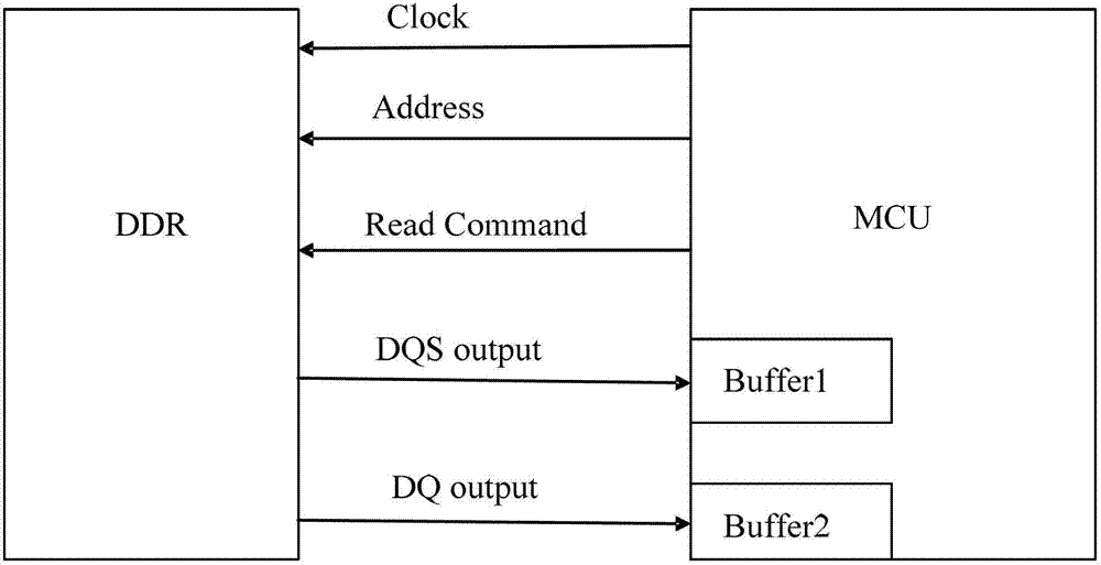
[0024] Such as figure 1 and figure 2 As shown, MCU (Micro Control Unit, micro control unit) includes Buffer 1 (buffer register 1) and Buffer 2 (buffer register 2), and MCU realizes DDR (Double Data Rate Synchronous Dynamic Random Access Memory, Double Data Rate Synchronous Dynamic Random Access Memory, double-rate synchronous dynamic random access memory) read and write operations. The MCU adjusts the phase of DQS (Data Strobe, data gate) by adjusting the value of Buffer 1, and the DQS is used to control data read and write operations. The MCU adjusts the phase of DQ (Data, data) by adjusting the value of Buffer 2.

[0025] Such as image 3 Shown is a functional block diagram of a preferred embodiment of the DDR debugging system of the present invention. The DDR debugging system 10 runs in the MCU, and the DDR d...


PUM


Abstract

The invention provides a method for debugging a double data rate synchronous dynamic random access memory (DDR SDRAM). According to the method, a data stroke (DQS) phase is adjusted through gradually adjusting the value of a Buffer 1, a data (DQ) phase is adjusted through gradually adjusting the value of a Buffer 2, and an adjusting cycle of the DQS phase and an adjusting cycle of the DQ phase are constructed through analyzing the working condition of the DDR SDRAM after the value of the Buffer 1 and the value of the Buffer 2 are adjusted, and further, the best operating point of the DDR SDRAM is found out, so that a DQS signal and a DQ signal are harmonious, and the phenomenon that an error occurs when a read operation is performed on the DDR SDRAM by a micro control unit (MCU) is avoided. The invention also provides a system for debugging the DDR SDRAM.

Description

technical field [0001] The invention relates to a device debugging technology, in particular to a DDR debugging method and system. Background technique [0002] The full name of DDR is: DDR SDRAM (Double Data Rate Synchronous Dynamic Random Access Memory, double rate synchronous dynamic random access memory). Due to the higher DDR read / write data speed, the timing and signal requirements are getting higher and higher. On the other hand, due to cost requirements, the size of PCB (Printed Circuit Board, printed circuit board) is getting smaller and smaller. The requirements for PCB layout design are getting higher and higher. It is difficult to make all the differential signal traces the same length, so there will be an equal difference delay between the signals. When the delay reaches a certain level, it will lead to the reading of the DDR. / Write operation fails, resulting in a crash, which poses a great challenge to the use of high-speed devices such as DDR. [0003] At p...

Claims


Application Information

Patent Timeline
Patent Type & Authority Applications(China)
IPC IPC(8): G06F11/26
Inventor 易山珍
Owner SHENZHEN TCL NEW-TECH CO LTD
Features
  • R&D
  • Intellectual Property
  • Life Sciences
  • Materials
  • Tech Scout
  • Unparalleled Data Quality
  • Higher Quality Content
  • 60% Fewer Hallucinations
Learn More