Vacuum casing for critical dimension scanning electron microscopy (CD-SEM)

An electron microscope and critical dimension technology, applied in the direction of discharge tubes, circuits, electrical components, etc., can solve the problems of damage to the positioning groove of the wafer to be tested, low hardness, and scrapping of the wafer to be tested, so as to improve the quality of shipments and reduce production. The effect of cost and simple structure

Active Publication Date: 2013-04-10
CSMC TECH FAB2 CO LTD
View PDF3 Cites 1 Cited by
  • Summary
  • Abstract
  • Description
  • Claims
  • Application Information

AI Technical Summary

Problems solved by technology

[0004] At present, wafers are usually made of silicon, germanium, or semiconductor materials containing silicon and / or germanium, which have physical characteristics such as low hardness and high brittleness. When pin contact is used to locate the wafer to be tested, the positioning groove of the wafer to be tested will usually be damaged to varying degrees, and in severe cases, the wafer to be tested will be scrapped, and the above situation will have a serious impact on the shipment quality of the batch of wafers

Method used


Image

  • Vacuum casing for critical dimension scanning electron microscopy (CD-SEM)

Examples


Embodiment Construction

[0019] In the following description, numerous specific details are given in order to provide a more thorough understanding of the present invention. It will be apparent, however, to one skilled in the art that the present invention may be practiced without one or more of these details. In other examples, some technical features known in the art are not described in order to avoid confusion with the present invention.

[0020] In order to provide a thorough understanding of the present invention, the detailed structure will be set forth in the following description. It is evident that the practice of the invention is not limited to specific details familiar to those skilled in the art. Preferred embodiments of the present invention are described in detail below, however, the present invention may have other embodiments besides these detailed descriptions.

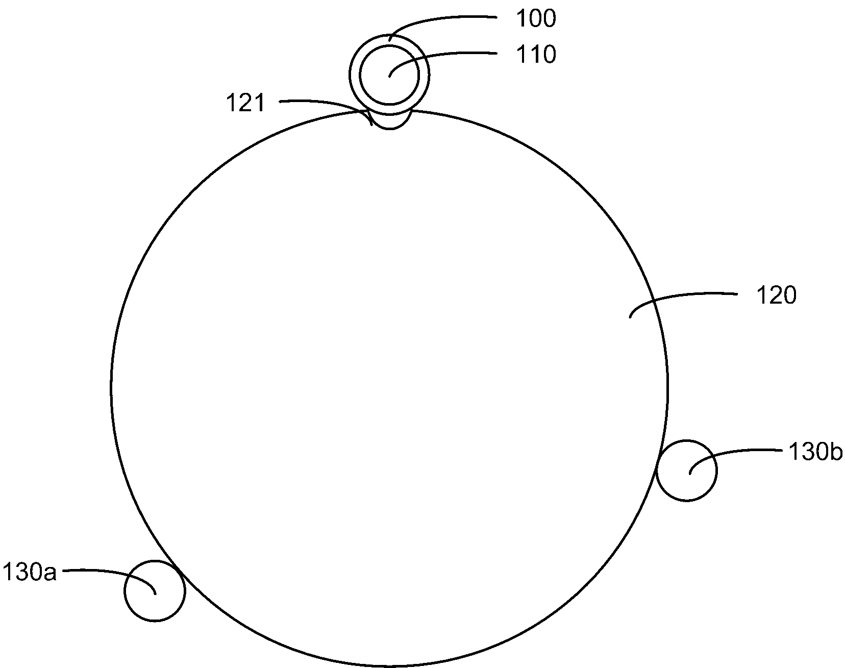
[0021] The invention provides a critical dimension scanning electron microscope. The stage of the critical dimension sc...


PUM


Abstract

The invention discloses a vacuum casing for a CD-SEM. The vacuum casing is in a ring structure, the inner diameter of the vacuum casing is matched with a pin arranged on a stage of the CD-SEM, and the hardness of the vacuum casing is smaller than that of a wafer to be tested. A notch at the edge of the wafer to the tested can be protected from being damaged through installing the vacuum casing on the notch pin of the CD-SEM, therefore the delivery quality of the wafer is improved, and the production cost is reduced. Additionally, the vacuum casing has the advantages of being simple in structure, convenient to install, easy to process and the like.

Description

technical field [0001] The invention relates to the field of semiconductors, in particular to a vacuum sleeve for a critical dimension scanning electron microscope and a critical dimension scanning electron microscope using the vacuum sleeve. Background technique [0002] In recent years, with the continuous reduction of critical dimensions of semiconductor devices, Critical Dimension Scanning Electron Microscopy (CD-SEM) has been widely used in the field of semiconductor device manufacturing to measure critical dimensions online. [0003] When using a critical dimension scanning electron microscope to measure the critical dimension of a semiconductor device, it is first necessary to transfer the wafer to be measured to a predetermined position on the stage and fix it at the predetermined position. At present, a critical dimension scanning electron microscope usually uses a mechanical device to perform positioning operations on the wafer to be tested. Taking HITACHI's criti...

Claims


Application Information

Patent Timeline
Patent Type & Authority Applications(China)
IPC IPC(8): H01J37/20H01J37/28
Inventor 刘伟王迪
Owner CSMC TECH FAB2 CO LTD
Why Eureka
Try Eureka