Stacking-type semiconductor package structure

A packaging structure and semiconductor technology, which is applied in the direction of semiconductor devices, semiconductor/solid-state device components, electric solid-state devices, etc., to achieve the effects of increasing qualification, enhancing heat dissipation, and avoiding interference with other effects

Inactive Publication Date: 2013-04-10
CHIPSIP TECH CO LTD +1
View PDF3 Cites 6 Cited by
  • Summary
  • Abstract
  • Description
  • Claims
  • Application Information

AI Technical Summary

Problems solved by technology

[0006] In view of this, the purpose of the present invention is to provide a stacked semiconductor packaging structure to solve the technical problem that the prior art cannot use three-dimensional packaging technology to form a packaging structure with multiple electronic functions

Method used


Image

  • Stacking-type semiconductor package structure
  • Stacking-type semiconductor package structure
  • Stacking-type semiconductor package structure

Examples


Embodiment Construction

[0056] The terms "first", "second" and "third" mentioned below are used to distinguish the referred elements, not to sort or limit the difference of the referred elements, and are not used to limit the scope of the invention. The term "circuit board" mentioned below at least includes a single-layer or multi-layer substrate and at least one conductive circuit. Conductive traces are formed on the outer surface of the substrate and / or the surface of the inner interlayer. Furthermore, the conductive lines can penetrate through one or more layers of the substrate to form electrical connections between different surfaces of the substrate.

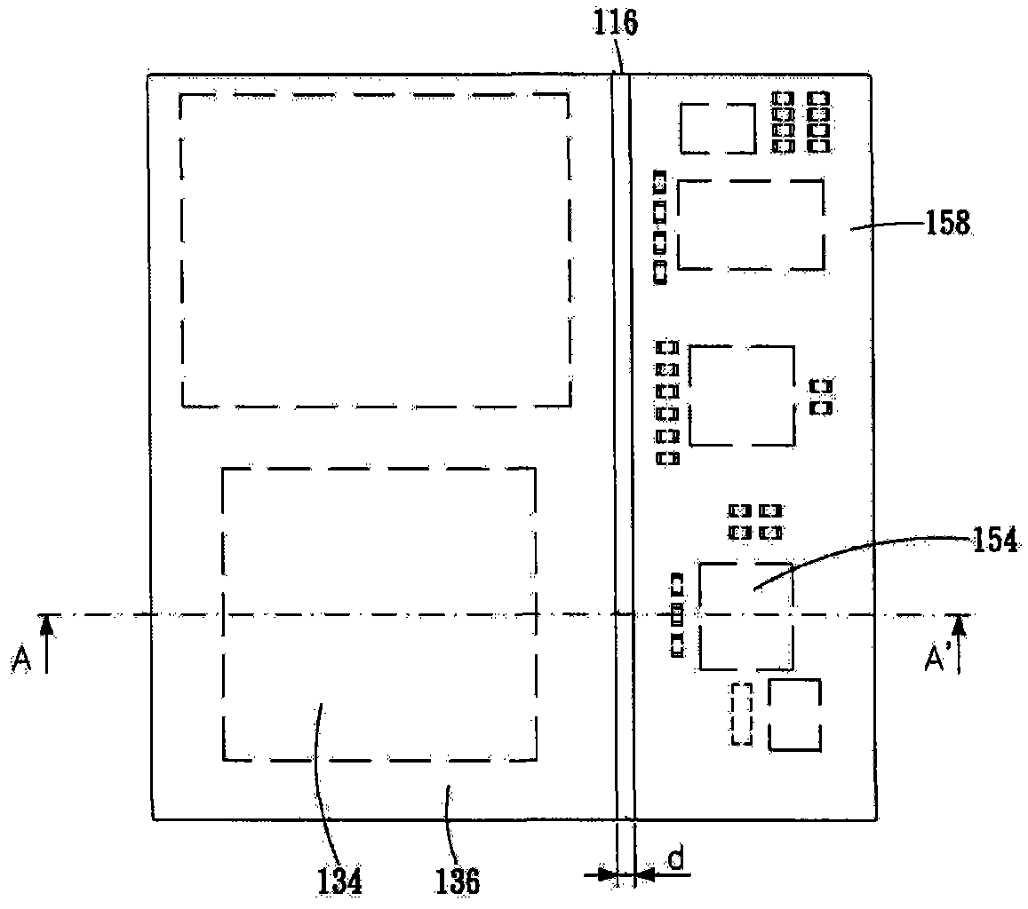
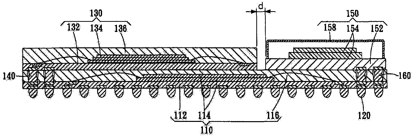
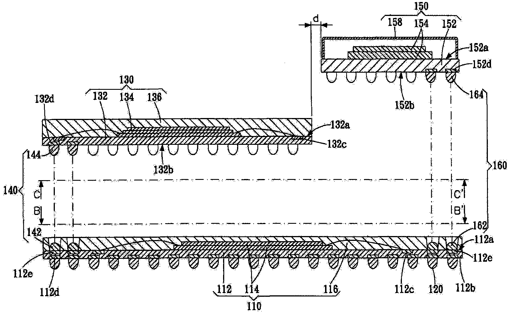
[0057] figure 1 It is a top view of a stacked semiconductor package structure according to an embodiment of the present invention, figure 2 yes figure 1 A schematic diagram of the cross-sectional structure of an embodiment along the tangent line A-A', and image 3 yes figure 2 An exploded view of an embodiment of the cross-sectional struc...


PUM


Abstract

A stacking-type semiconductor package structure includes a first package body, multiple first connecting conductors, a second package body, multiple second connecting conductors, an electronic function module, and multiple third connecting conductors. The first connecting conductors are disposed on a lower surface of the first package body and connected electrically to the first package body. The second package body and the electronic function module are disposed on an upper surface of the first package body. The second connecting conductors are connected electrically between the first package body and the second package body, and the third connecting conductors are connected electrically between the first package body and the electronic function module. The second package body has an electronic function different from that of the electronic function module.

Description

technical field [0001] The invention relates to a package structure, in particular to a stacked semiconductor package structure. Background technique [0002] With the trend of short, light and thin electronic products, the circuit board inside is also getting smaller and smaller, so that the area on which components can be placed on the circuit board is also reduced. In the past, multiple chips could be directly bonded to the circuit board in a side-by-side manner, but this is gradually impossible to achieve in advanced miniaturized electronic products. Therefore, a plurality of chips are vertically stacked, which is called a semiconductor package stacking device (Package-On-Package device; POP). Here, different chip stacks are integrated on the same substrate by using a surface mount technology (SMT) process, so as to meet the requirements of small bonding area and high-density device arrangement. [0003] Moreover, with the sharp increase in the demand for functions and...

Claims


Application Information

Patent Timeline
Patent Type & Authority Applications(China)
IPC IPC(8): H01L25/00H01L23/31H01L23/367H01L23/552
CPCH01L23/3128H01L23/36H01L23/3677H01L23/49816H01L23/49838H01L23/552H01L24/73H01L25/105H01L25/50H01L2224/32225H01L2224/48227H01L2224/73265H01L2225/0651H01L2225/06568H01L2225/1005H01L2225/1023H01L2225/1058H01L2225/1094H01L2924/15311H01L2924/15331H01L2924/3025H01L2924/00012H01L2924/00
Inventor 周儒聪
Owner CHIPSIP TECH CO LTD
Why Eureka
Try Eureka