Grid structure of multi-layer film and manufacturing method of grid structure

A manufacturing method and gate structure technology, applied in the direction of electrical components, circuits, semiconductor devices, etc., can solve the problems of non-disclosure and achieve the effect of reducing the depression

Inactive Publication Date: 2013-04-10
SHANGHAI HUAHONG GRACE SEMICON MFG CORP
View PDF4 Cites 0 Cited by
  • Summary
  • Abstract
  • Description
  • Claims
  • Application Information

AI Technical Summary

Problems solved by technology

This patent application is helpful to the leakage problem of gate oxide, but due to the limitation of the process in the scheme, especially the amorphous silicon deposited on the first layer of film cannot be processed at high temperature before the etching is completed (the formation of crystals of a certain size affects the reverse etching effect) is not disclosed, nor is there any disclosure about better blocking the diffusion of phosphorus in the second layer by depositing some oxide after the first layer

Method used


Image

  • Grid structure of multi-layer film and manufacturing method of grid structure
  • Grid structure of multi-layer film and manufacturing method of grid structure
  • Grid structure of multi-layer film and manufacturing method of grid structure

Examples


Embodiment 1

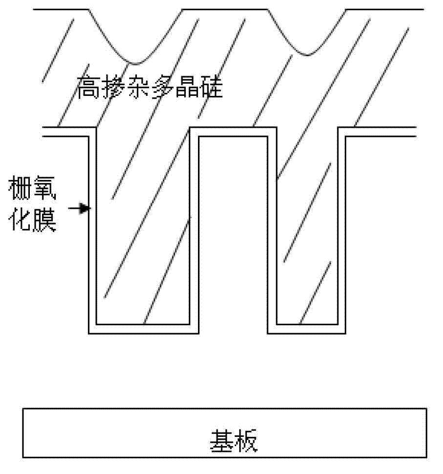
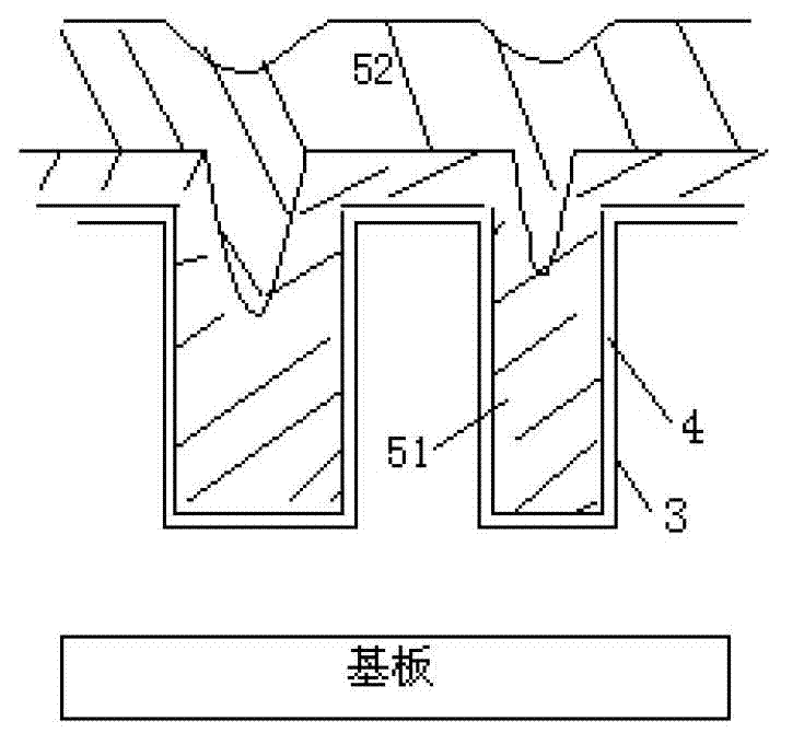
[0028] see image 3 , 4 As shown, the gate structure of the multilayer film includes: a gate oxide 4 formed in the trench 3; a first layer of polysilicon or amorphous silicon 51 with a high phosphorus doping concentration on the gate oxide 4, the first layer The phosphorus doping concentration of layer polysilicon or amorphous silicon 51 is 1E20-10E20atm / cm 3 , with a thickness of 3,000 angstroms to 10,000 angstroms; on the first layer of polysilicon or amorphous silicon 51, a second layer of polysilicon or amorphous silicon 52 with low phosphorous doping concentration, the second layer of polysilicon or amorphous silicon 52 The phosphorus doping concentration of the first layer of amorphous silicon or polysilicon 51 is less than or equal to 1 / 2 times of the phosphorus doping concentration of the first layer of amorphous silicon or polysilicon 51 .

[0029] The manufacturing method of the gate structure of the above-mentioned multilayer film, its processing step comprises: ...

Embodiment 2

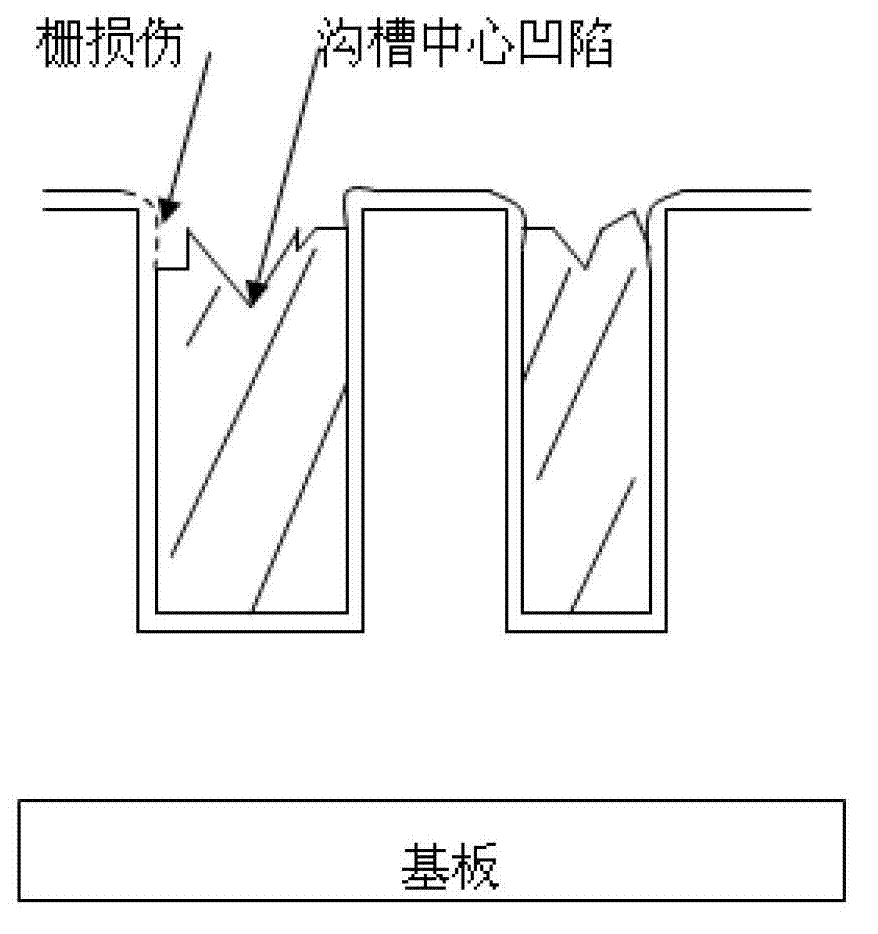
[0035] see Figure 5 , the difference between this embodiment and Embodiment 1 is that after step 3 is completed, when the upper end surface of the second layer of polysilicon or amorphous silicon 52 is the lowest (see Figure 5 The dotted line at "C" in ) is higher than the gate oxide 4 on both ends of the trench 3 (see Figure 5 When the dotted line at "D" in the above), the third layer of polysilicon or amorphous silicon 53 with lower phosphorus doping concentration or no phosphorus doping is filled; then, dry etching is used to remove the polysilicon on the surface of the silicon wafer Or the amorphous silicon is completely etched away to obtain a gate structure filled with polysilicon or amorphous silicon in the trench (see Figure 6 ).

Embodiment 3

[0037] see Figure 7 , the difference between this embodiment and Embodiment 1 is that after step 2 is completed, when the upper end surface of the first layer of polysilicon or amorphous silicon 51 is the lowest (see Figure 7 The dotted line at "E" in ) is higher than the gate oxide 4 line on both ends of trench 3 (see Figure 7"F" in the dotted line), and then deposit the second layer of polysilicon or amorphous silicon 52.

[0038] In the above three embodiments, the polysilicon or amorphous silicon at the top position of the edge of the trench 3 may have a recess 61 after etching back, which will damage the gate oxide at the edge of the trench 3, so it can be etched back when necessary. After the completion, at least one gate oxide repair is performed, usually at a temperature higher than 1000°C. Diffusion process, rapid oxidation or annealing process can be used; the damage of gate oxide 4 exposed at the top of the edge of trench 3 can be repaired, thereby improving the...


PUM


Abstract

The invention discloses a grid structure of a multi-layer film. The grid structure comprises grid oxygen formed in a groove, a first layer of polycrystalline silicon or amorphous silicon and a second layer of polycrystalline silicon or amorphous silicon. The first layer of polycrystalline silicon or amorphous silicon is arranged above the grid oxygen and contains high-concentration phosphorus. The concentration of the contained phosphorus of the first layer of polycrystalline silicon or amorphous silicon is 1-10*10<20> atm/cm<3>. The second layer of polycrystalline silicon or amorphous silicon which contains low-concentration phosphorus is arranged above the first layer of polycrystalline silicon or amorphous silicon. The concentration of the contained phosphorus of the second layer of polycrystalline silicon or amorphous silicon is equal to or smaller than half of the concentration of the contained phosphorus of the first layer of polycrystalline silicon or amorphous silicon. The invention further discloses a manufacturing method of the grid structure of the multi-layer film. The electricity leakage characteristic of the grid oxygen can be improved, and performance of devices can be improved.

Description

technical field [0001] The invention relates to the field of semiconductor integrated circuits, in particular to a multilayer film gate structure. The present invention also relates to a manufacturing method of the gate structure. Background technique [0002] In the current semiconductor process method, there is such a process method that first forms a trench on the silicon wafer, and then oxidizes to form a layer of oxide film as a gate oxide film (hereinafter referred to as "gate oxide"), and then grows A layer of highly doped polysilicon or amorphous silicon doped with phosphorus, filling the entire trench with highly doped polysilicon or amorphous silicon (see figure 1 ). After the entire trench is filled, etch back, all the highly doped polysilicon or amorphous silicon without the trench is etched away, and the highly doped polysilicon or amorphous silicon left in the trench is used as The gate, and the amorphous silicon will become polysilicon after the subsequent ...

Claims


Application Information

Patent Timeline
Patent Type & Authority Applications(China)
IPC IPC(8): H01L29/423H01L21/28
Inventor 肖胜安
Owner SHANGHAI HUAHONG GRACE SEMICON MFG CORP
Why Eureka
Try Eureka