Press fit method for to-be-pressed multi-layer plate with chip window

A multi-layer board and window technology, applied in the direction of multi-layer circuit manufacturing, etc., can solve problems such as failure to meet application requirements, and achieve the effects of avoiding product scrapping, improving force uniformity, and improving yield

Active Publication Date: 2015-05-06
JIANGNAN INST OF COMPUTING TECH
View PDF5 Cites 0 Cited by
  • Summary
  • Abstract
  • Description
  • Claims
  • Application Information

AI Technical Summary

Problems solved by technology

[0005] In practice, it is found that the above method cannot effectively bond multilayer boards with chip windows, and cannot meet the requirements of the application.

Method used


Image

  • Press fit method for to-be-pressed multi-layer plate with chip window
  • Press fit method for to-be-pressed multi-layer plate with chip window
  • Press fit method for to-be-pressed multi-layer plate with chip window

Examples


Embodiment Construction

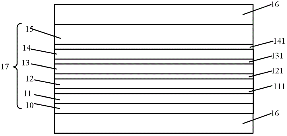
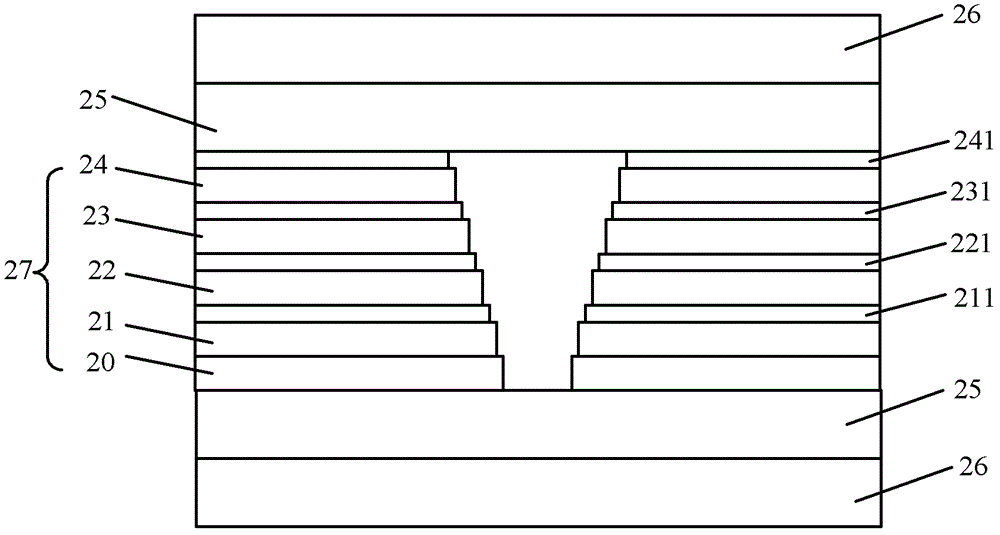
[0034] Please refer to the lamination principle of the existing multi-layer board with chip window figure 2 shown. The multi-layer board 27 to be laminated in the figure includes a plurality of single-layer boards stacked, which are respectively:

[0035] The first prepreg 21; the first wiring layer 211 located on the first prepreg 21 (the first prepreg 21 and the first wiring layer 211 form a first single-layer board); located on the first wiring layer 211 The second prepreg 22 on the top; the second wiring layer 221 on the second prepreg 22 (the second prepreg 22 and the second wiring layer 221 form a second single-layer board); The third prepreg 23 on the second wiring layer 221; the third wiring layer 231 on the third prepreg 23 (the third prepreg 23 and the third wiring layer 231 constitute a third single-layer board ); the fourth prepreg 24 on the third wiring layer 231; the fourth wiring layer 241 on the fourth prepreg 24 (the fourth prepreg 24 and the fourth wiring ...


PUM


Abstract

An embodiment of the invention provides a press fit method for a to-be-pressed multi-layer plate with a chip window. The press fit method comprises providing the to-be-pressed multi-layer plate, a hard lining plate, two heat conducting pressure transmitting plates and a soft lining plate, enabling the to-be-pressed multi-layer plate to comprise a plurality of single-layer plates formed by stacking, and enabling the chip window to be formed in the to-be-pressed multi-layer plate; arranging stuffing in the chip window, and enabling the shape and the dimensions of the stuffing to correspond to the dimensions of the chip window; enabling the soft lining plate, the to-be-pressed multi-layer plate, the hard lining plate and one heat conducting pressure transmitting plate to be sequentially placed on the other heat conducting pressure transmitting plate, and enabling the stuffing to be located in the chip window; enabling the heat conducting pressure transmitting plates and the to-be-pressed multi-layer plate to be pressed into an integrated multi-layer plate; and removing the heat conducting pressure transmitting plate, the soft lining plate and the stuffing above the integrated multi-layer plate and the hard lining plate and the heat conducting pressure transmitting plate below the integrated multi-layer plate. The press fit method solves the problem that the multi-layer plate with the chip window cannot be stressed evenly during press fit.

Description

technical field [0001] The invention relates to the field of manufacturing PCB substrates, in particular to a pressing method for a multilayer board to be pressed with a chip window. Background technique [0002] The PCB substrate is usually a multi-layer board. In the existing multi-layer boards, the single-layer boards are usually made first, and then the single-layer boards are stacked, and the single-layer boards are pressed into a multi-layer board by pressing. Specifically, please refer to figure 1 , is a schematic diagram of the lamination principle of the existing multi-layer board. The laminated multi-layer board 17 includes a plurality of stacked single-layer boards, each single-layer board includes a prepreg, and at least one side of the prepreg is formed with a wiring layer, which are: the first prepreg 11, the material is a prepreg, and the A first wiring layer 111 is formed on the first prepreg 11 (the first prepreg 11 and the first wiring layer 111 form a fi...

Claims


Application Information

Patent Timeline
Patent Type & Authority Patents(China)
IPC IPC(8): H05K3/46
Inventor 吴梅珠刘秋华吴小龙梁少文陈文录徐杰栋穆敦发胡广群
Owner JIANGNAN INST OF COMPUTING TECH
Why Eureka
Try Eureka