Nonvalatile memory device and programming method and memory device system including the nonvalatile memory device

A non-volatile storage and line memory technology, which is applied in the field of semiconductor storage devices and can solve problems such as lost data

Active Publication Date: 2013-04-17
SAMSUNG ELECTRONICS CO LTD
View PDF7 Cites 36 Cited by
  • Summary
  • Abstract
  • Description
  • Claims
  • Application Information

AI Technical Summary

Problems solved by technology

[0005] Volatile memory devices can lose st...

Method used


Image

  • Nonvalatile memory device and programming method and memory device system including the nonvalatile memory device
  • Nonvalatile memory device and programming method and memory device system including the nonvalatile memory device
  • Nonvalatile memory device and programming method and memory device system including the nonvalatile memory device

Examples


Embodiment Construction

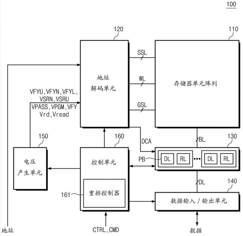
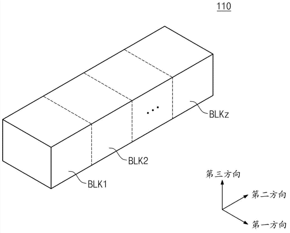
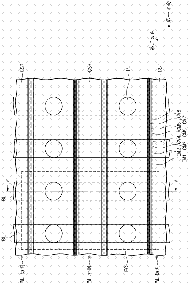
[0116]Various exemplary embodiments will be described more fully hereinafter with reference to the accompanying drawings, in which some exemplary embodiments are shown. However, this invention may be embodied in many different forms and should not be construed as limited to the exemplary embodiments set forth herein. These exemplary embodiments are merely examples, and many implementations and variations are possible that do not require the details presented here. It should also be emphasized that this disclosure provides details of alternative examples, but this list of alternatives is not exhaustive. Furthermore, any consistency of details between the various examples should not be construed as requiring such details—it would be unfeasible to list every possible variation for every feature described here. Reference should be made to the language of the claims when determining the requirements of the invention. In the drawings, the size and relative sizes of layers and regi...


PUM


Abstract

Disclosed are a programming method and a nonvalatile memory device. The method includes receiving programming data to be programmed in a memory device unit; reading the memory device unit to determine an erasure state and at least one programming state; executing state reading operation, wherein the at least one programming state is used by a plurality of states to read voltage; and reading operation results according to states and using a plurality of verification voltage with different levels to program programming data in the memory device unit. Also disclosed is a method for using a plurality of verification voltage, in which verification voltage is selected based on other characteristic elements which can influence threshold voltage offset or represent data of the memory device unit after programming.

Description

[0001] Cross References to Related Applications [0002] This application claims priority from Korean Patent Application No. 10-2011-0104753 filed on Oct. 13, 2011, which is hereby incorporated by reference in its entirety. technical field [0003] The inventive concepts described herein relate to semiconductor memory devices, and more particularly, to methods of programming nonvolatile memory devices and memory systems including the same. Background technique [0004] Semiconductor memory devices may be manufactured using semiconductors such as silicon (Si), germanium (Ge), gallium arsenide (GaAs), indium phosphide (InP), and the like. Semiconductor memory devices are classified into volatile memory devices and nonvolatile memory devices. [0005] Volatile memory devices may lose stored data when they are turned off or lose power. Volatile memory devices include static RAM (SRAM), dynamic RAM (DRAM), synchronous DRAM (SDRAM), and others. Nonvolatile memory devices retain...

Claims


Application Information

Patent Timeline
IPC IPC(8): G11C16/06G11C16/02
CPCG11C16/12G11C11/5628G11C16/0483G11C16/3418G11C16/3454H10B41/27H10B43/27
Inventor 郭东勋朴相元郑原宅
Owner SAMSUNG ELECTRONICS CO LTD
Why Eureka
Try Eureka