Liquid crystal display device

A liquid crystal display device, display area technology, applied in nonlinear optics, instruments, optics, etc., can solve the problems of increasing manufacturing cost, prolonging manufacturing time, not fully utilizing the area of ​​Cs lines, etc., shortening manufacturing time, and increasing pixel openings The effect of increasing the effective light transmission area area

Inactive Publication Date: 2013-04-24
NANJING CEC PANDA LCD TECH
View PDF4 Cites 17 Cited by
  • Summary
  • Abstract
  • Description
  • Claims
  • Application Information

AI Technical Summary

Problems solved by technology

Replacing the metal Cs line with a transparent conductive layer can increase the pixel aperture ratio by omitting the Cs line, but the transparent conductive layer itself is not 100% transparent. If ITO is used as the transparent conductive layer, the light transmittance is generally around 90%-93%. , so this FFS structure does not fully utilize the area of ​​the original Cs line
Moreover, since the transparent conductive layer needs to use special film formation, photolithography, and etching processes, the manufacturing cost is increased and the manufacturing time is prolonged.

Method used


Image

  • Liquid crystal display device
  • Liquid crystal display device
  • Liquid crystal display device

Examples


Embodiment Construction

[0038] Below in conjunction with accompanying drawing and specific embodiment, further illustrate the present invention, should be understood that these embodiments are only for illustrating the present invention and are not intended to limit the scope of the present invention, after having read the present invention, those skilled in the art will understand various aspects of the present invention Modifications in equivalent forms all fall within the scope defined by the appended claims of this application.

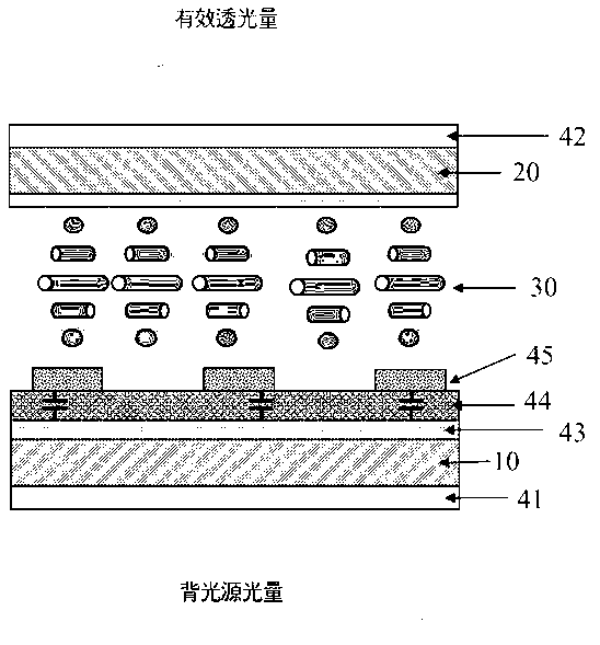
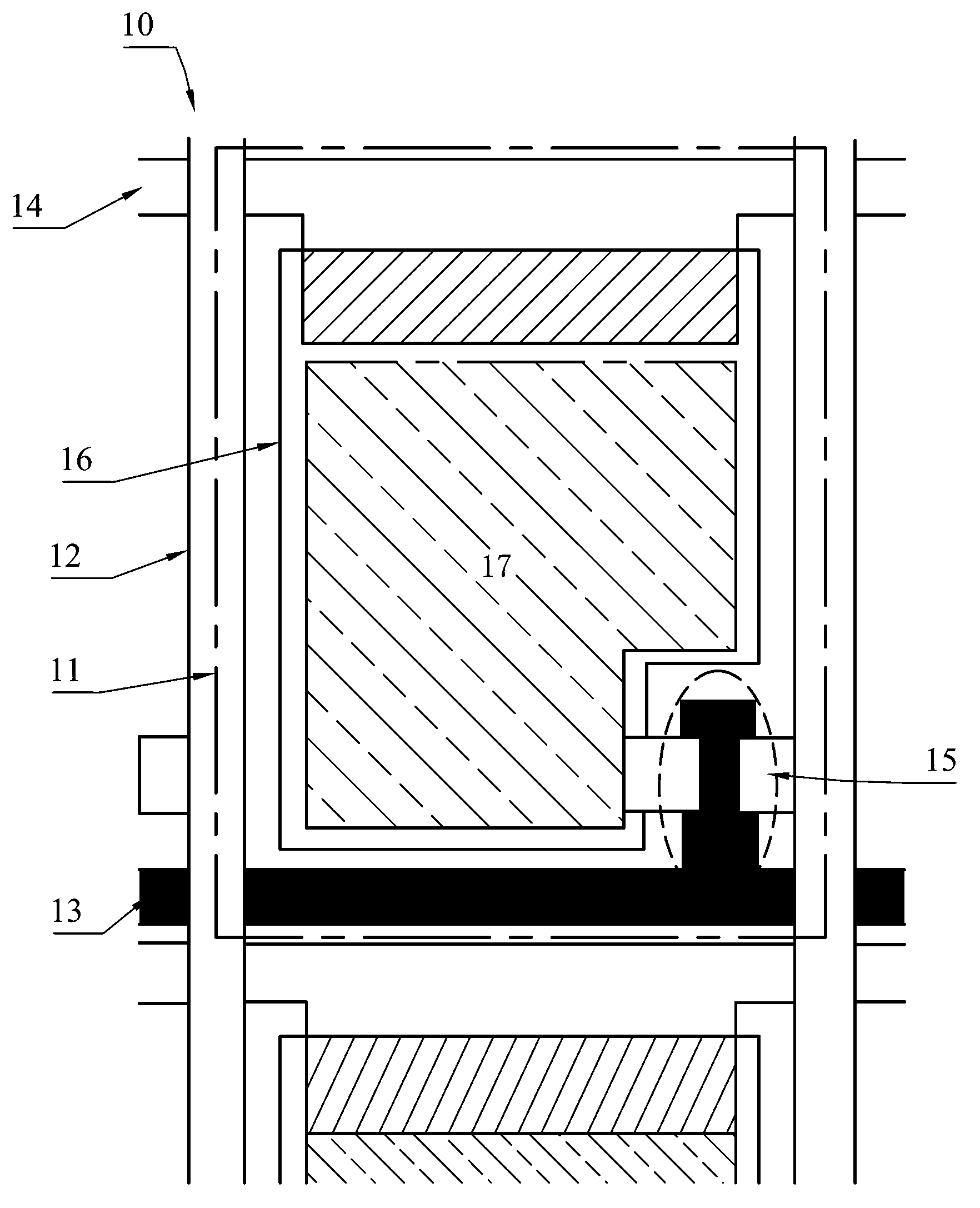
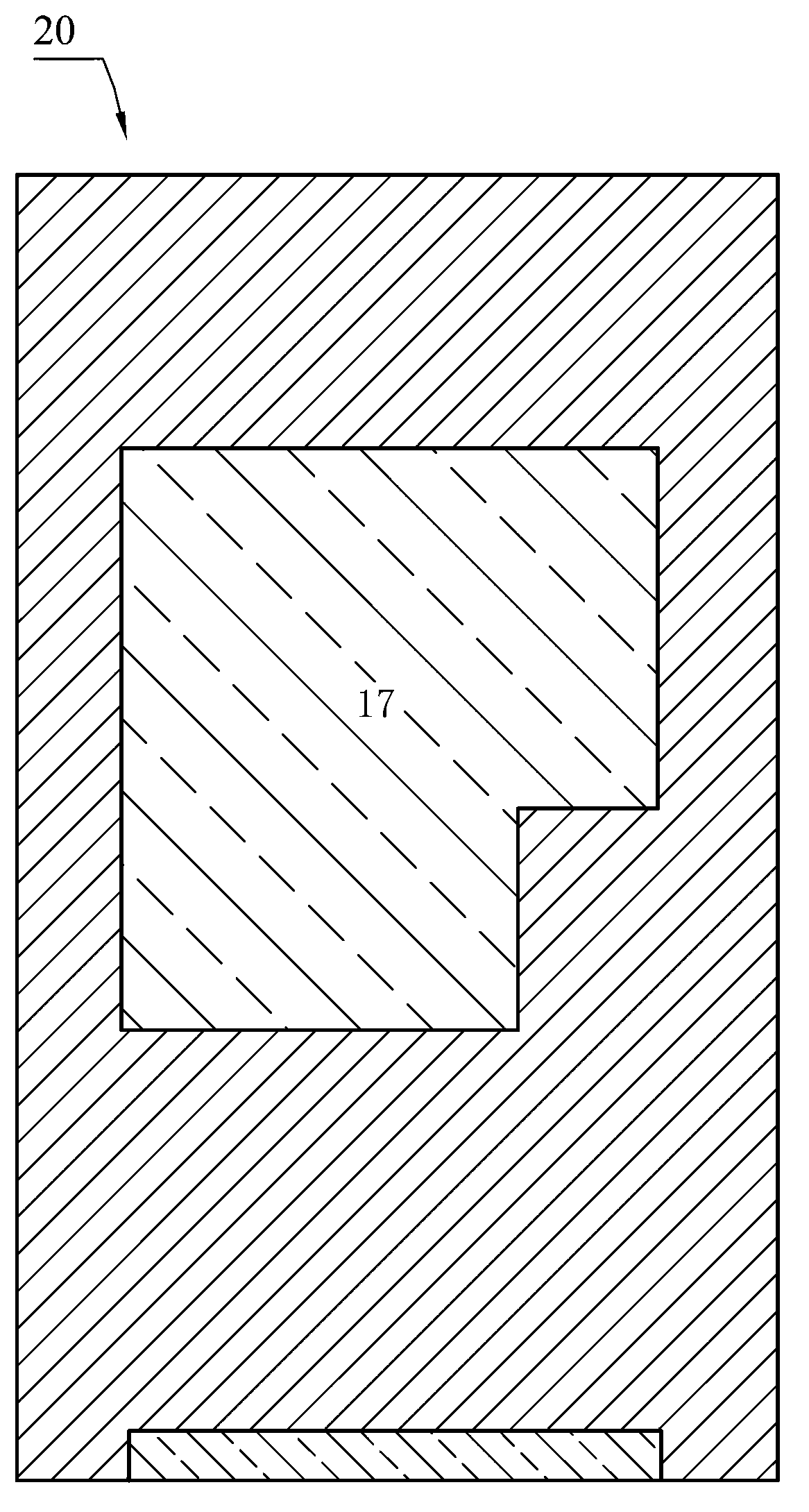
[0039] Figure 6 to Figure 8 It is a structural schematic diagram of the first embodiment of the liquid crystal display device of the present invention, such as Figure 8 As shown, the liquid crystal display device includes an opposite first substrate 10, a second substrate 20, a liquid crystal layer interposed between the first substrate 10 and the second substrate 20, and a liquid crystal layer supported on the first substrate 10 or the second substrate 20. A number of ...


PUM

PropertyMeasurementUnit
transmittivityaaaaaaaaaa

Abstract

The invention provides a liquid crystal display device which comprises a first substrate, a second substrate, and a liquid crystal layer. The first substrate is opposite to the second substrate. The liquid crystal layer is stuck between the first substrate and the second substrate. The first substrate comprises a pixel electrode and a first alignment film. The first alignment film, which is opposite to the second substrate, is arranged on the pixel electrode. The second substrate comprises at least one support pillar, a transparent conducting layer and a second alignment film. The support pillar is coated with the transparent conducting layer. The second alignment film, which is opposite to the first substrate, is arranged on the transparent conducting layer. The first alignment film attaches to the second alignment film on the support pillar. According to the design, the support pillar is coated with the pixel electrode or the transparent conducting layer without designing special storage capacitance lines on the first substrate and without widening the width of scanning lines. The liquid crystal display device can not only increase the pixel opening ratio substantially and improve effective light-permeating area, but also shorten manufacture time and lower manufacture cost.

Description

technical field [0001] The invention relates to a liquid crystal display device with high light transmittance. Background technique [0002] The luminance of the liquid crystal display device is the product of the luminance of the backlight source and the transmittance of the pixels. Under the premise that the luminance of the liquid crystal display device is constant, increasing the transmittance of the pixels can reduce the brightness of the backlight source, thereby realizing energy saving and consumption reduction. Increasing the pixel aperture ratio, liquid crystal transmission efficiency, polarizer transmittance, and color filter transmittance can increase the pixel transmittance. Among them, increasing the pixel aperture ratio is the most common and most effective method. [0003] Such as figure 1 with figure 2 Shown is a schematic plan view of an existing common liquid crystal display device. The existing liquid crystal display device includes a first substrate 1...

Claims


Application Information

Patent Timeline
Patent Type & Authority Applications(China)
IPC IPC(8): G02F1/1337G02F1/1343G02F1/1362G02F1/1339
Inventor 马群刚
Owner NANJING CEC PANDA LCD TECH
Why Eureka
Try Eureka