
Complementary metal oxide semiconductor (CMOS) band-gap reference circuit based on negative feedback

A reference circuit and negative feedback technology, applied in the direction of adjusting electrical variables, control/regulating systems, instruments, etc., can solve the problems of large chip area, complex reference structure, and unsatisfactory cost performance. Simple structure, good temperature coefficient effect

Active Publication Date: 2013-04-24
拓尔微电子股份有限公司
View PDF6 Cites 28 Cited by
  • Summary
  • Abstract
  • Description
  • Claims
  • Application Information

AI Technical Summary

Problems solved by technology

[0006] However, these solutions often only optimize one of the temperature drift or PSRR indicators while ignoring the other indicator, and cannot take into account both indicators at the same time; or the designed reference structure is more complicated, which increases the difficulty of integrated circuit design and occupies the chip. The area is too large, the price / performance ratio is not very ideal

Method used


Image

  • Complementary metal oxide semiconductor (CMOS) band-gap reference circuit based on negative feedback
  • Complementary metal oxide semiconductor (CMOS) band-gap reference circuit based on negative feedback
  • Complementary metal oxide semiconductor (CMOS) band-gap reference circuit based on negative feedback

Examples


Embodiment Construction

[0018] In order to make the object, technical solution and advantages of the present invention clearer, the present invention will be further described in detail below in conjunction with the accompanying drawings and specific embodiments. The specific embodiments described here are only used to explain the present invention, not to limit the present invention.

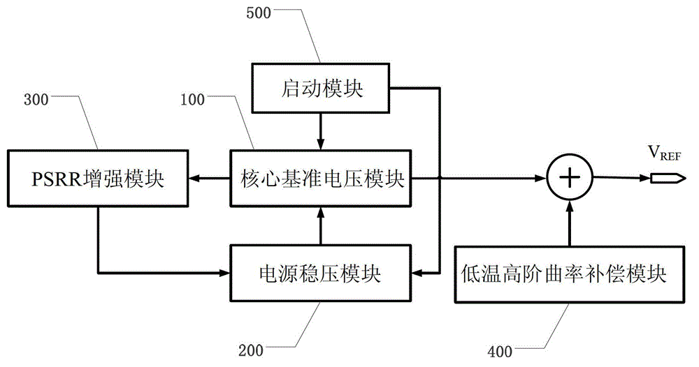
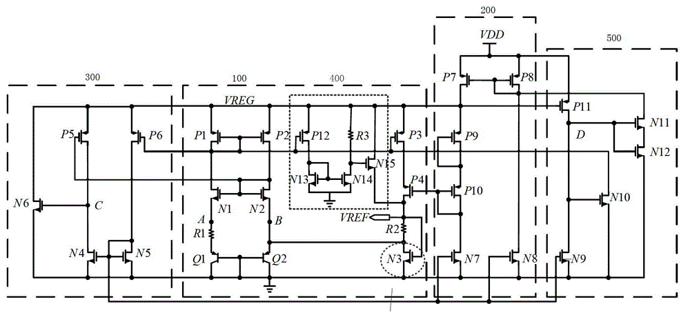
[0019] Such as figure 1 As shown, the embodiment of the present invention is provided with a core reference voltage module 100 with negative feedback, a power supply voltage stabilization module 200, a PSRR enhancement module 300, a low-temperature high-order curvature compensation module 400, and a startup module 500; the core reference with negative feedback The voltage module 100 generates a bandgap reference voltage, and its output terminals are respectively connected to the input terminals of the PSRR enhancement module 300 and the low-temperature high-order curvature compensation module 400; the power supply vol...


PUM


Abstract

A complementary metal oxide semiconductor (CMOS) band-gap reference circuit based on negative feedback relates to an integrated circuit. The circuit is provided with a core reference voltage module with negative feedback, a power supply stabilizing module, a power supply rejection ratio (PSRR) reinforcing module, a low temperature high order curvature compensation module and a starting module. The core reference voltage module with the negative feedback generates band-gap reference voltage, and the output end of the core reference voltage module with the negative feedback is respectively connected with the input ends of the PSRR reinforcing module and the low temperature high order curvature compensation module. The power supply stabilizing module provides a stabling power supply to other modules, and the output end of the power supply stabilizing module serves as the power supply input ends of other modules. The output end of the PSRR reinforcing module is connected with the power supply input ends of the core reference voltage module with the negative feedback, the power supply stabilizing module, the low temperature high order curvature compensation module and the starting module. The output end of the low temperature high order curvature compensation module is connected with the output end of the core reference voltage module with the negative feedback and outputs final reference voltage. The output end of the starting module is respectively connected with the core reference voltage module with the negative feedback and the power supply stabilizing module.

Description

technical field [0001] The invention relates to integrated circuits, in particular to a CMOS bandgap reference circuit based on negative feedback. Background technique [0002] In the design of analog circuits and digital-analog hybrid integrated circuits, it is often necessary to use a reference voltage source, which converts the power supply voltage into a reference voltage independent of the power supply voltage and temperature, and is used to provide stable bias and reference voltages for other parts of the circuit. Therefore, the low temperature drift coefficient and high voltage rejection ratio are the key performance indicators of the bandgap reference source. The CMOS bandgap reference voltage also needs to be compatible with the CMOS process and be easily integrated into an integrated circuit chip of the CMOS process. [0003] The traditional bandgap reference voltage uses the base-emitter voltage V BE and a thermal voltage V with a positive temperature coefficien...

Claims


Application Information

Patent Timeline
IPC IPC(8): G05F1/567
Inventor 李晓潮林昱林春郭东辉
Owner 拓尔微电子股份有限公司
Learn More