Serial Peripheral Interface (SPI) controller and communication method

A controller and control register technology, applied in the field of serial communication, can solve the problems of increasing the burden of software designers, increasing software overhead and CPU resource occupation, and achieving the effect of reducing software control and improving utilization rate

Active Publication Date: 2013-04-24
SUZHOU ZHONGKE ADVANCED TECH RES INST CO LTD
3 Cites 22 Cited by

AI-Extracted Technical Summary

Problems solved by technology

[0023] Therefore, regardless of whether the SPI controller is configured as a master or a slave, after the receiving data buffer is full of data, regardless of whether the received data is actually used, the data in the receiving data buffer mus...

Abstract

The invention relates to a Serial Peripheral Interface (SPI) controller. The controller comprises an inner bus interface module, a register module, a data converting module, a state and breaking control module, a data transmitting and receiving buffer and a state limiting machine which is used for generating output of Slave Select (SS) and SPI Clock (SCLK) in accordance with SPI transmitting parameters for controlling the storage of the register and SCLK Baud rate parameters for controlling the storage of a Baud rate register in the register module. For the modified SPI controller, the SS output is controlled by SPI controller hardware automatically when the controller is a host computer, and the software is not required to simulate the SS output, when the reading of the data in the buffer is selected, the unnecessary operation that a Central Processing Unit (CPU) reads and receives the data buffer is reduced, the required software control is reduced greatly when the CPU operates the SPI controller, and the use rate of the CPU is improved.

Application Domain

Technology Topic

Image

  • Serial Peripheral Interface (SPI) controller and communication method
  • Serial Peripheral Interface (SPI) controller and communication method
  • Serial Peripheral Interface (SPI) controller and communication method

Examples

  • Experimental program(1)

Example Embodiment

[0062] The present invention will be further described in detail below with reference to the accompanying drawings and specific embodiments.
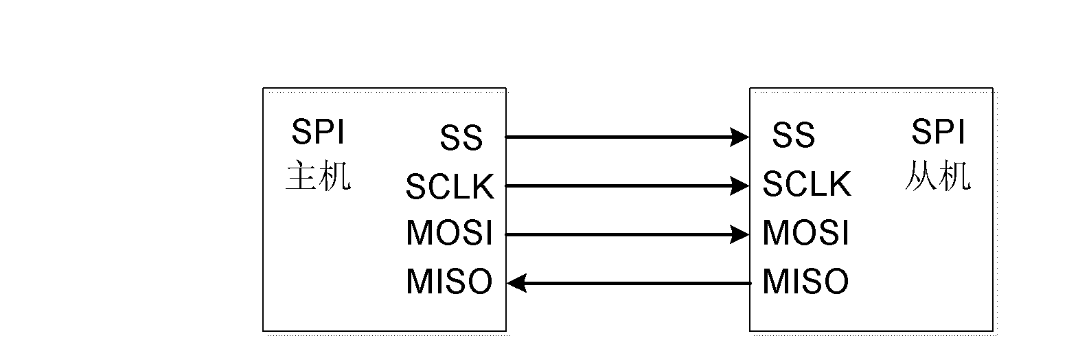
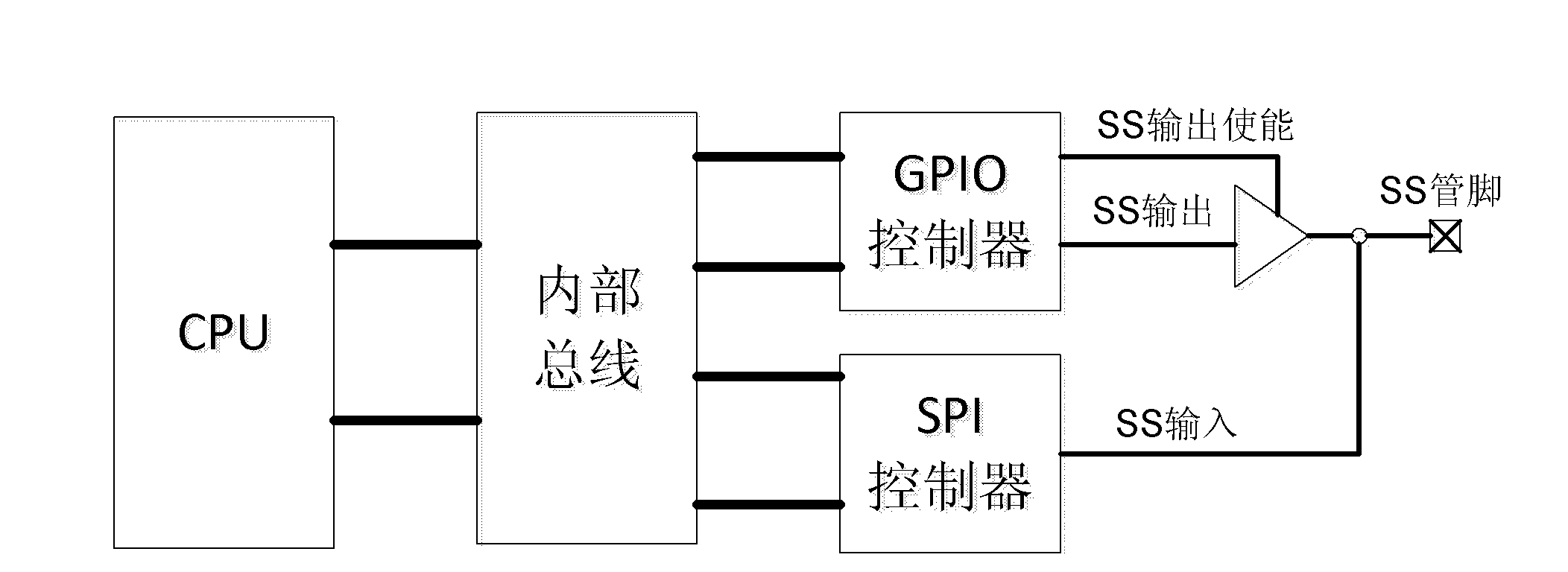
[0063] The present invention provides an SPI controller, such as Figure 4 As shown, it includes an internal bus interface module, which is used to realize the CPU operation of the SPI controller and the register module through the internal bus, and receives the configuration of the SPI controller from the CPU transmitted through the internal bus interface module, and a data conversion module for outputting data in parallel The conversion and input data serial-to-parallel conversion, state and interrupt control module is used to report the state of the SPI controller and generate interrupts, and it is characterized in that it also includes a finite state machine, which is used for according to the SPI transmission parameters registered by the control register in the register module and The SCLK baud rate parameter registered in the baud rate register generates SS and SCLK outputs; the transmit and receive data buffers are used to buffer the data to be transmitted and received, respectively; the above-mentioned finite state machine includes idle, start, transmission and end four state.
[0064] like Figure 5 As shown, it is a schematic diagram of the connection of the SS end of the SPI controller. The CPU1 is connected to the SPI controller 3 through the internal bus 2. The SPI controller controls the SS to work as follows:
[0065] 1) When the CPU configures the SPI controller as a slave: the SPI controller hardware automatically configures the SS pin as an input and connects to the SS output of the external SPI master. In this state, only when the SS input is low, the SPI control The device communicates with the external SPI host;
[0066] 2) When the CPU configures the SPI controller as the host:
[0067] a) When it is a single SPI host system, there is no need to detect MODF (Mode Fault, mode error: that is, multiple SPI hosts operate the SPI bus at the same time), the CPU configures the SPI controller to not enable MODF, that is, MODFEN=0), SPI control The hardware of the controller automatically configures the SS pin as an output, and the SS output level is controlled by the SPI controller hardware according to the SPI transmission parameters, such as CPHA (Clock Phase, clock phase) and CPOL (Clock Polarity, clock polarity);
[0068] b) When it is a multi-SPI host system, MODF needs to be detected, the CPU configures the SPI controller to enable MODF, that is, MODFEN=1, the SPI controller hardware automatically configures the SS pin as an input, and the SPI controller detects the SS input: if the SS input is Low level, there are other SPI masters operating the SPI bus, the SPI controller hardware is automatically configured as a slave, and reports MODF to the CPU; on the contrary, if the SS input is high, no other SPI masters are operating the SPI bus, The SPI controller can work in the host mode, and then the CPU configures the SPI controller to disable MODF, that is, MODFEN=0, the SPI controller hardware automatically configures the SS pin as an output, and the SS output level is determined by the SPI controller according to the SPI transmission parameter hardware. Control, the above transmission parameters such as CPHA and CPOL.
[0069] like Image 6 As shown, it is a transition diagram of a finite state machine, and the above finite state machine includes four states: idle, start, transfer and end.
[0070] The improved SPI controller provided by the present invention, 1) when it is configured as a host, the SS output is completely controlled automatically by the SPI controller hardware, without software to control the analog SS output, 2) the data in the received data buffer can be read Optionally, unnecessary operations of the CPU to read and receive data buffers are reduced, and software control required when the CPU operates the SPI controller is reduced, thereby improving the utilization rate of the CPU.
[0071] Further, the above-mentioned SPI controller also includes a sending data buffer and a receiving data buffer, and the above-mentioned receiving data buffer is used to buffer the data received by the SPI controller; the above-mentioned receiving data buffer is controlled as follows: the data in the receiving data buffer After the storage is full, when new data is written into the receive data buffer, the data written first is overwritten by the data after the data written first, and so on, the data before the data written last is overwritten by the data written last. The data is overwritten, thereby forming a data space to store the new data written.
[0072] like Figure 7As shown, the working principle of the SPI controller receiving data buffer of the present invention is that there is no data in the initial receiving data buffer, which is in an empty state, and then the written data is stored in the corresponding position in turn. It is assumed that the maximum capacity of the receiving data buffer is N, after storing N pieces of data, the received data buffer is full of data and is in a full state. If the SPI controller receives new data and writes it into the receive data buffer, at this time, data 1 will overwrite the first written data 0, and similarly, data 2 overwrites data 1, and so on, data N overwrites data N-1 , which will create a space at address N that can be used to store the new data written. Therefore, the first-in first-out is guaranteed, and after the data is full, new data is written and the previously written data is overwritten.
[0073] In the improved SPI controller provided by the present invention, the reading of the data in the received data buffer is optional: if there is a practical purpose, read it away, otherwise, the read operation may not be performed, so that the subsequently received data will be automatically overwritten. The data that has been written in the receiving data buffer reduces unnecessary operations of the CPU to read the receiving data buffer, and at the same time reduces the software control required when the CPU operates the SPI controller, thereby improving the CPU utilization.
[0074] Further, the above-mentioned data conversion module includes an output data parallel-to-serial conversion unit and an input data serial-to-parallel conversion unit, and the above-mentioned output data parallel-to-serial conversion unit is used to read the parallel data in the transmission data buffer and output after parallel-serial conversion, wherein , when the SPI controller is configured as a master, it outputs to the MOSI signal line; on the contrary, when the SPI controller is configured as a slave, it outputs to the MISO signal line; the above-mentioned input data serial-parallel conversion unit is used to convert the input serial data After serial-to-parallel conversion, the received data buffer is written. When the SPI controller is configured as a master, the input is the MISO signal line; on the contrary, when the SPI controller is configured as a slave, the input is the MOSI signal line.
[0075] Further, the above-mentioned register module includes a control register and a baud rate register, the above-mentioned control register is used for receiving and registering the CPU configuration SPI transmission parameters; the above-mentioned baud rate register is used for receiving and registering the CPU configuration SCLK clock baud rate parameter.
[0076] Among them, the above transmission parameters include SPIE (SPI Enable, SPI enable), MSS (Master Slave Select, master-slave selection: '1' as master, '0' as slave), CPHA, CPOL, MODFEN (mode error enable) and DataSize (data bit width selection: '00' means 8-bit, '01' means 16-bit, '10' means 32-bit).
[0077] The above status and interrupt control module is used to report the working status of the SPI controller and generate interrupts, including TxFIFOEmpty (transmit data buffer empty flag), TxFIFOFull (transmit data buffer full flag), RxFIFOEmpty (receive data buffer empty flag) , RxFIFOFull (receive data buffer full flag) and MODF.
[0078] The SPI controller can support different combinations of CPHA and CPOL transfer parameters, support 8-bit, 16-bit and 32-bit data transfer, and support MSB first transfer MLFS=1 or LSB first transfer MLFS=0. Among them, MLFS (MSB LSB First Select, high and low bit selection: '1' means the MSB First highest bit is transmitted first, and '0' means the LSB First lowest bit is transmitted first).
[0079] Another aspect of the present invention also provides a communication method for the SPI controller for the SPI controller, comprising:
[0080] S1, the system is reset, the finite state machine is in an idle state, SS outputs a high level, and the SCLK output is CPOL;
[0081] S2. The CPU configures the SPI controller as the host MSS=1, disables MODF (MODFFEN=0), enables the SPI controller (SPIEN=1), the SPI controller is the host and waits for SPI transmission;
[0082] S3. The CPU writes the data to be transmitted into the transmit data buffer, and the write operation will start the SPI transmission: the SPI controller detects that there is data in the transmit data buffer (TxFIFOEmpty=0), reads the data in the transmit data buffer and starts SPI transmission;
[0083] S4. The finite state machine remains in an idle state. When it is detected that the count up counter is ClockNumber/2-1, the finite state machine is in the starting state, and the SS output is low to start the SPI transmission;
[0084] S5. The finite state machine maintains the starting state. When the up-counter counts to ClockNumber/2-1, the SCLK output flips to generate the SCLK clock output, and the SS outputs a low level, ClockNumber (baud rate value);
[0085] S6, the finite state machine is in the transmission state until the end of the data transmission, and enters the end state;
[0086] Further, it also includes,
[0087] S7. The finite state machine remains in the end state until the counter counts up to ClockNumber/2-1, and then the finite state machine performs state transition:
[0088] S8, such as Figure 8 As shown, when CPHA=0, the finite state machine enters the idle state, and SS outputs a high level and ends the current SPI transmission, waiting for the next SPI transmission;
[0089] S9, such as Figure 9 As shown, when CPHA=1, if there is still data in the transmit data buffer, the finite state machine enters the transmission state, and at the same time keeps the SS output low to start the next SPI transmission; otherwise, if there is no data in the transmit data buffer, The finite state machine enters the idle state, and at the same time SS outputs a high level and ends the current SPI transfer, waiting for the next SPI transfer.
[0090] Among them, the above SPI transmission is:
[0091] S10, the CPU configures the SPI controller as the host, and judges the type of the SPI host system;
[0092] S11. When it is a multi-SPI host system, MODF needs to be detected. The CPU configures the SPI controller to enable MODF, and the SPI controller configures SS as the input and detects the SS input level:
[0093] SS is low level, and there are other SPI masters operating the SPI bus. At this time, the SPI controller hardware is automatically configured as a slave and reports MODF to the CPU;
[0094] SS is high level, there is no other SPI master to operate the SPI bus, the SPI controller can be configured as the master and start SPI transmission, the CPU configures the SPI controller to disable MODF, the SPI controller configures SS as the output, and prepares for SPI transmission;
[0095] When it is a single SPI host system, the CPU configuration does not enable MODF, the SPI controller configures SS as the output, and prepares for SPI transmission;
[0096] S12. The CPU writes the baud rate register to configure the SCLK baud rate parameter; SCLK clock frequency = system clock frequency/value of the baud rate register, where the lowest bit is always 0, that is, the value of the baud rate register is even, and the system The clock frequency is the operating frequency of the internal bus interface clock connected to the SPI controller.
[0097] S13. The CPU write operation control register configures the SPI transmission parameters, such as CPHA and CPOL;
[0098] S14. The CPU writes the data to be transmitted into the sending data buffer; the data conversion module reads out the data in the sending data buffer, performs parallel-serial conversion, and outputs it to MOSI, and at the same time performs serial-to-parallel conversion on the input MISO and writes it to the receiving data buffer;
[0099] S15, continuous SPI controller data transmission;
[0100] S16. When there is still data in the sending data buffer, it is necessary to continue the transmission and perform step S14, and start the next transmission, otherwise, the transmission ends.
[0101] S17, the CPU reads the data received in the receiving data buffer. Wherein, step S17 can be selectively applied; steps S10-S17 are the flow of the CPU operating the SPI controller to realize the SPI transmission.
[0102] The specific embodiments of the present invention described above do not limit the protection scope of the present invention. Any other corresponding changes and modifications made according to the technical concept of the present invention shall be included in the protection scope of the claims of the present invention.

PUM

no PUM

Description & Claims & Application Information

We can also present the details of the Description, Claims and Application information to help users get a comprehensive understanding of the technical details of the patent, such as background art, summary of invention, brief description of drawings, description of embodiments, and other original content. On the other hand, users can also determine the specific scope of protection of the technology through the list of claims; as well as understand the changes in the life cycle of the technology with the presentation of the patent timeline. Login to view more.

Similar technology patents

Method for preparing polypeptide fruit jelly

InactiveCN1864528AEasy to carryIncrease usageVegetable proteins working-upNutrientBoiling point
Owner:CHINA RES INST OF DAILY CHEM IND

Floating leisure platform

InactiveUS20060162637A1Increase usageIncrease attractivenessLife-buoysRaftsMarine engineeringIngested food
Owner:ZEUS

Classification and recommendation of technical efficacy words

Why Eureka
Try Eureka