Wafer Map display model and application method thereof

A wafer and model technology, applied in special data processing applications, instruments, electrical digital data processing, etc., can solve problems such as inflexibility, poor portability, and weak function of the wafer Map display model, achieving high flexibility and good flexibility Sexuality, the effect of convenient working state

Inactive Publication Date: 2013-04-24
THE 45TH RES INST OF CETC
View PDF4 Cites 12 Cited by
  • Summary
  • Abstract
  • Description
  • Claims
  • Application Information

AI Technical Summary

Problems solved by technology

[0004] The purpose of the present invention is to provide a multi-functional wafer Map display model and its usage method in order to overcome the shortcomings in the prior art, aiming to solve the problem that the existing wafer Map display model is weak in function, poor in portability and not flexible enough to adapt to different changing problems

Method used


Image

  • Wafer Map display model and application method thereof
  • Wafer Map display model and application method thereof
  • Wafer Map display model and application method thereof

Examples


Embodiment Construction

[0043] In order to make the object, technical solution and advantages of the present invention clearer, the present invention will be further described in detail below in conjunction with the accompanying drawings.

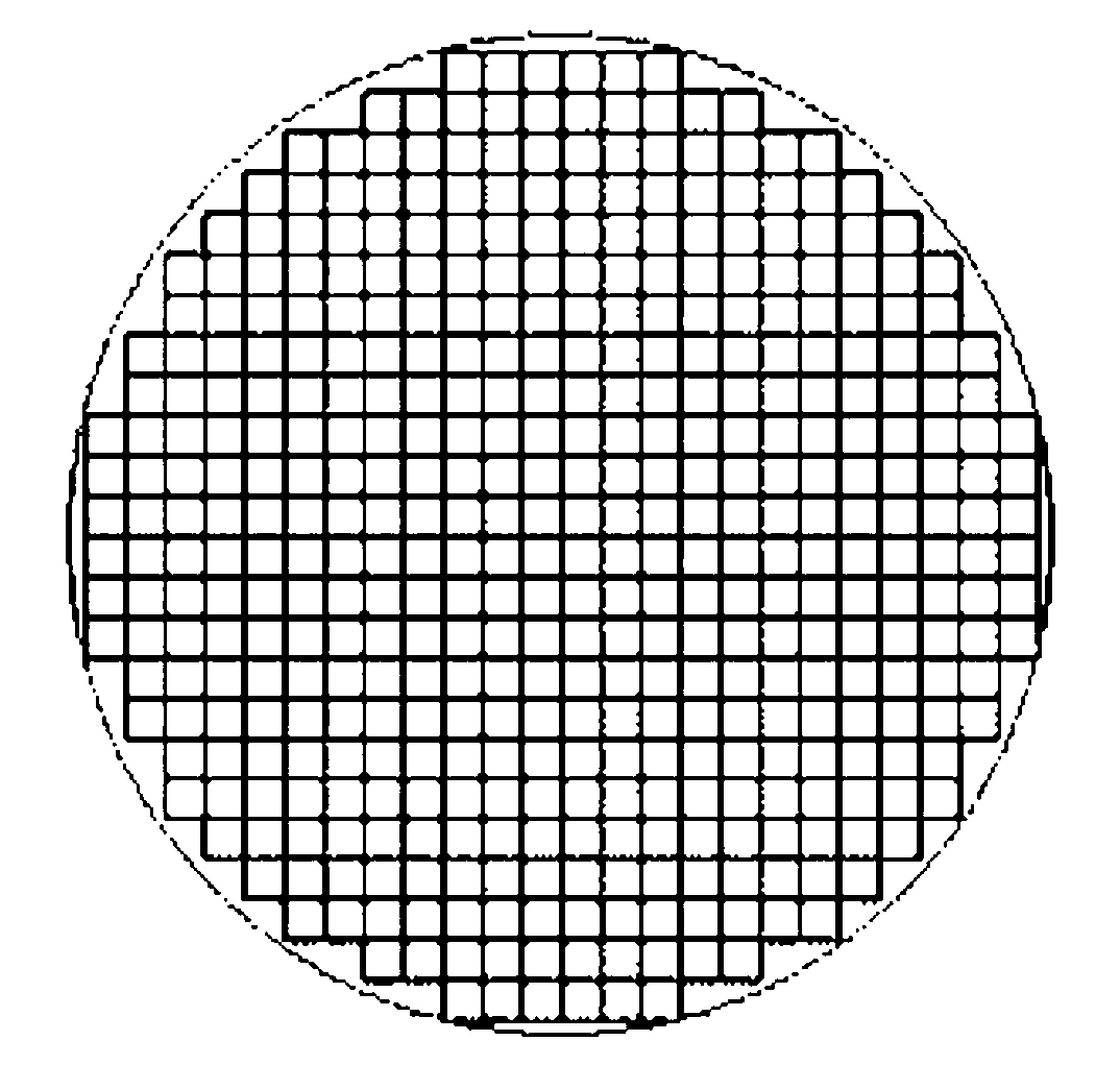
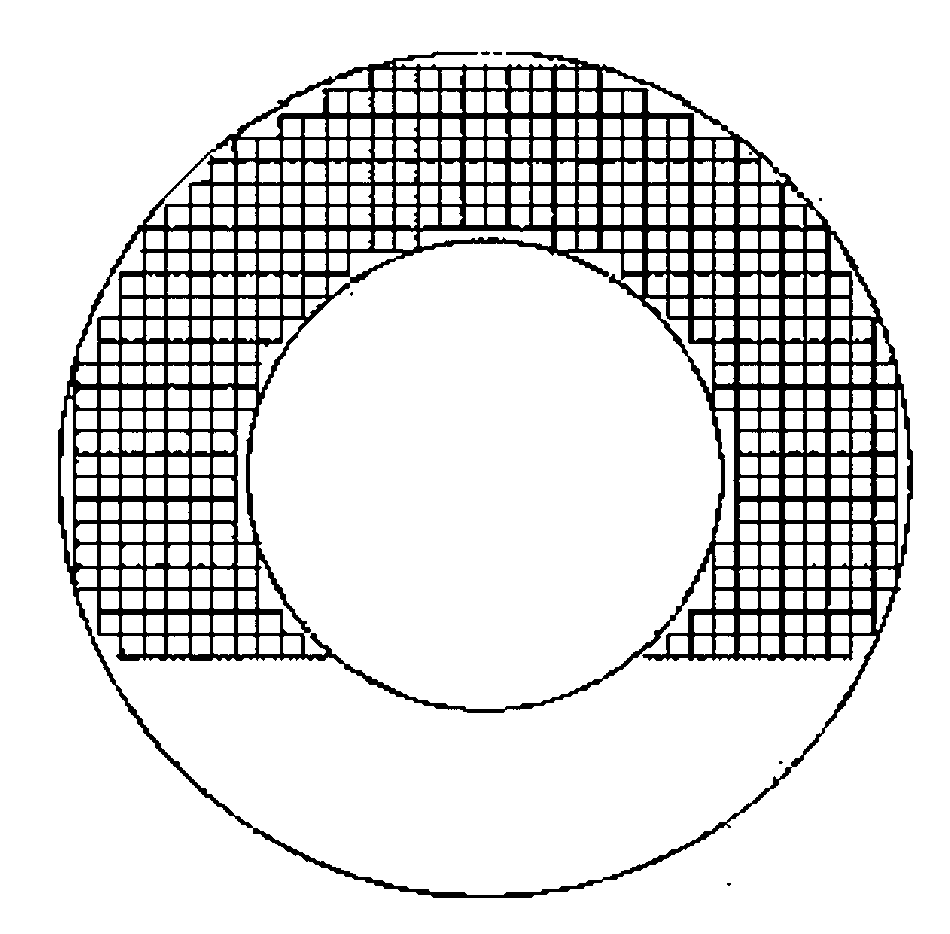
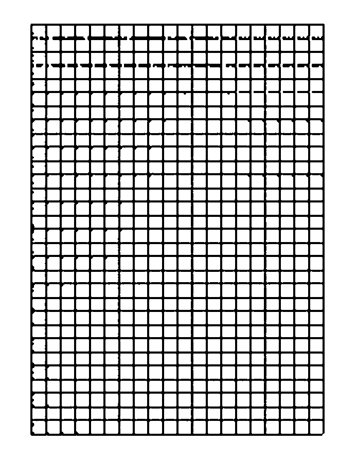
[0044] The invention utilizes configurable parameters to draw a wafer map to simulate the grain distribution on the wafer, and the color, shape and size of the wafer map can be set.

[0045] The model of the present invention is packaged into a dynamic link library, so that the upgrade of the model is convenient without affecting other parts of the system using the model. In addition, there is no restriction on which programming language the system uses, and it can be flexibly called by different languages. When using it, you only need to include the dynamic link library in the system that needs to use the model, create a new Map object, and call related functions to simulate and display the test status of the wafer in real time.

[0046] The creation process ste...


PUM


Abstract

The invention provides a wafer Map display model and an application method thereof. The method includes: building a dynamic linking library WaferMapDll firstly, building a derived class CWaferMap based on CStatic, building a wafer Map coordinate model, regarding each crystal grain as a point, and distributing a coordinate for each crystal grain; judging whether the distributed coordinates are in the range of a wafer, drawing small checks representing inner crystal grains of the wafer according to the crystal grains in the range of the wafer, and forming a wafer Map display image; building a binary file for storing crystal grain information and zoomed redrawn crystal grain test conditions, calculating a storage address of the information of each crystal grain in the file, and writing the crystal grain information in the file; obtaining a motor pulse coordinate of a current crystal grain, calculating a Map coordinate of a current crystal grain according to the motor pulse coordinate and a wafer central motor pulse coordinate, and marking and storing the corresponding crystal grains displayed on a Map image in the binary file. The wafer Map display model and the application method of the wafer Map display model are multifunctional, strong in portability and high in flexibility.

Description

technical field [0001] The invention relates to the technical field of semiconductor device testing, in particular to a wafer Map display model in probe testing equipment and a method for using the same. Background technique [0002] In the probe test equipment, it is necessary to display wafer information in real time, including the distribution status of the die on the wafer, whether the wafer has trimming, the position of the die currently being tested, and the classification level of the tested die, etc. the [0003] At present, each probe test equipment manufacturer has its own wafer map display model with similar basic functions. However, these models are weak in function, poor in portability, and not flexible enough to adapt to different changes. Contents of the invention [0004] The purpose of the present invention is to provide a multi-functional wafer Map display model and its usage method in order to overcome the shortcomings in the prior art, aiming to solve...

Claims


Application Information

Patent Timeline
Patent Type & Authority Applications(China)
IPC IPC(8): G06F17/50
CPCY02T10/82
Inventor 罗杨田洪涛刘国敬
Owner THE 45TH RES INST OF CETC
Why Eureka
Try Eureka