Low temperature co-fired ceramic (LTCC) double-layer microstrip antenna used for system-in-package
A technology of system-level packaging and microstrip antennas, which is applied in antennas, resonant antennas, antenna grounding devices, etc., can solve the problems of limited practical application and narrow impedance bandwidth, and achieve the effect of diversified functions, large bandwidth, and small size
- Summary
- Abstract
- Description
- Claims
- Application Information
AI Technical Summary
Problems solved by technology
Method used
Image

Examples
Embodiment 1
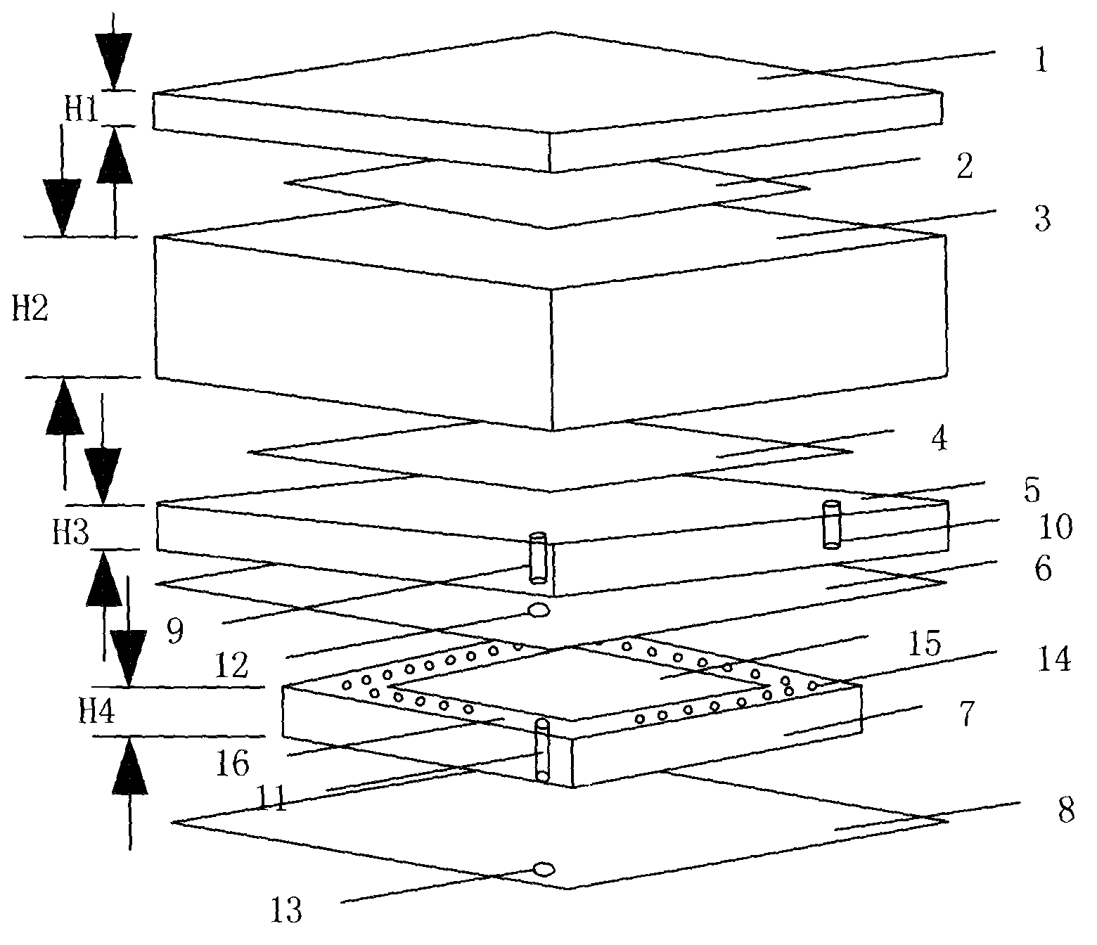
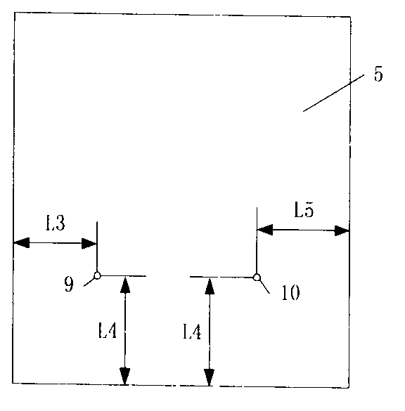
[0027] refer to figure 1 , the system of the present invention includes eight layers, the first layer is the antenna coating 1, the second layer is the upper radiation unit 2, the third layer is the middle interlayer 3, the fourth layer is the lower radiation unit 4, and the fifth layer is the antenna substrate layer 5. The sixth layer is the internal ground plane 6 , the seventh layer is the package body 7 , and the eighth layer is the external ground plane 8 . Among them: the first layer of antenna coating 1 is made of LTCC dielectric material with a thickness of H=0.79mm and a dielectric constant of 7.8, and the third interlayer 3 is made of an LTCC dielectric material with a thickness of H=3.3mm and a dielectric constant of 7.8 The fifth antenna substrate layer 5 is made of LTCC dielectric material with a thickness of H=1.03 mm and a dielectric constant of 7.8. The lower surface of the fifth layer is coated with silver or gold as the internal grounding metal layer 6; the ...
Embodiment 2
[0033] General structure is identical with embodiment 1, and its different parameters are as follows:
[0034] The thickness of the antenna coating 1 is H1 = 0.83 mm.
[0035] Antenna substrate 5 thickness H3=1.32mm
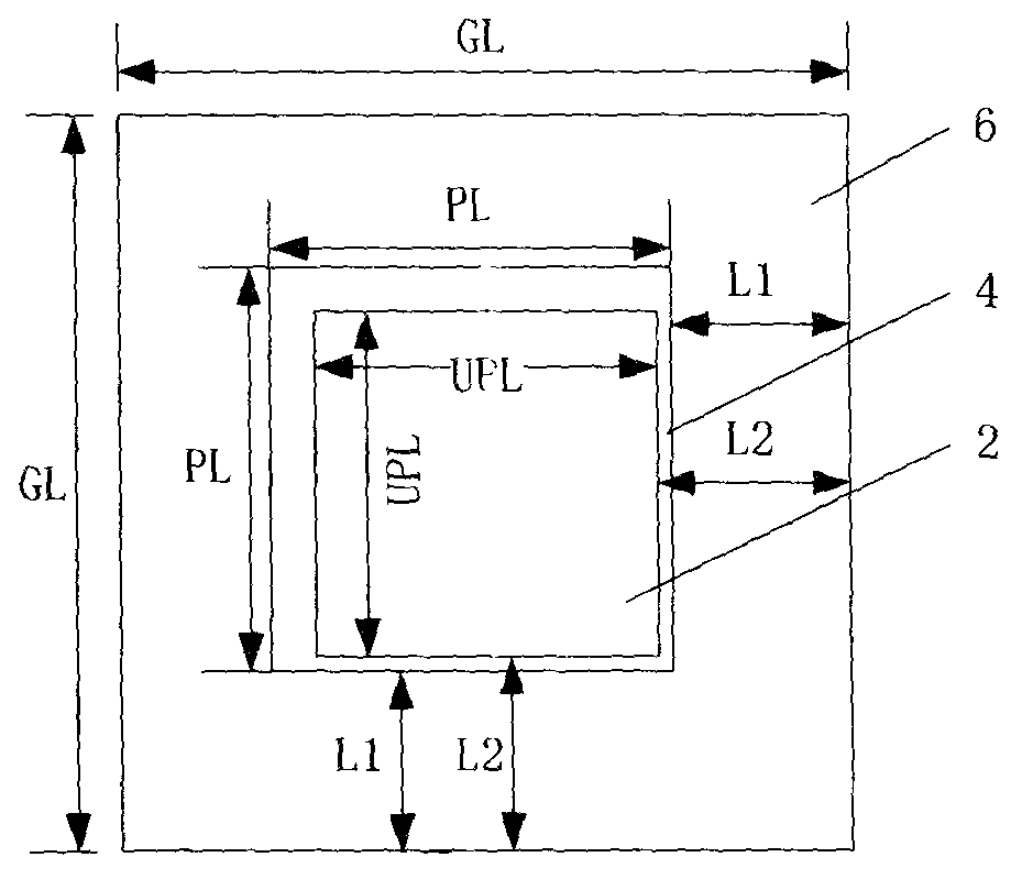
[0036]The upper radiating unit of the square sheet and the lower radiating unit of the square sheet adopt a coaxial design, and the central axes are on the same straight line, that is, the distance between the upper radiating unit 2 and the boundary of the middle interlayer 3 is L1=13.2mm, and the distance between the lower radiating unit 4 and the boundary of the middle interlayer 3 It is L2=13.9mm.
[0037] The thickness W1 of each side wall of the package body is 2 mm, and the distance between the through holes is 0.8 mm.
PUM
| Property | Measurement | Unit |
|---|---|---|
| Thickness | aaaaa | aaaaa |
| Thickness | aaaaa | aaaaa |
| Thickness | aaaaa | aaaaa |
Abstract
Description
Claims
Application Information
 - R&D Engineer
- R&D Manager
- IP Professional
- Industry Leading Data Capabilities
- Powerful AI technology
- Patent DNA Extraction
Browse by: Latest US Patents, China's latest patents, Technical Efficacy Thesaurus, Application Domain, Technology Topic.
© 2024 PatSnap. All rights reserved.Legal|Privacy policy|Modern Slavery Act Transparency Statement|Sitemap