OLED (Organic Light Emitting Diode) pixel structure and display device
A light-emitting diode and pixel structure technology, which is applied to static indicators, instruments, semiconductor devices, etc., can solve problems such as high synchronization requirements for timing control chips and differences in sub-blocks, so as to improve RC delay problems, improve display uniformity, Guarantee the effect of display quality
- Summary
- Abstract
- Description
- Claims
- Application Information
AI Technical Summary
Problems solved by technology
Method used
Image
Examples
Embodiment 1
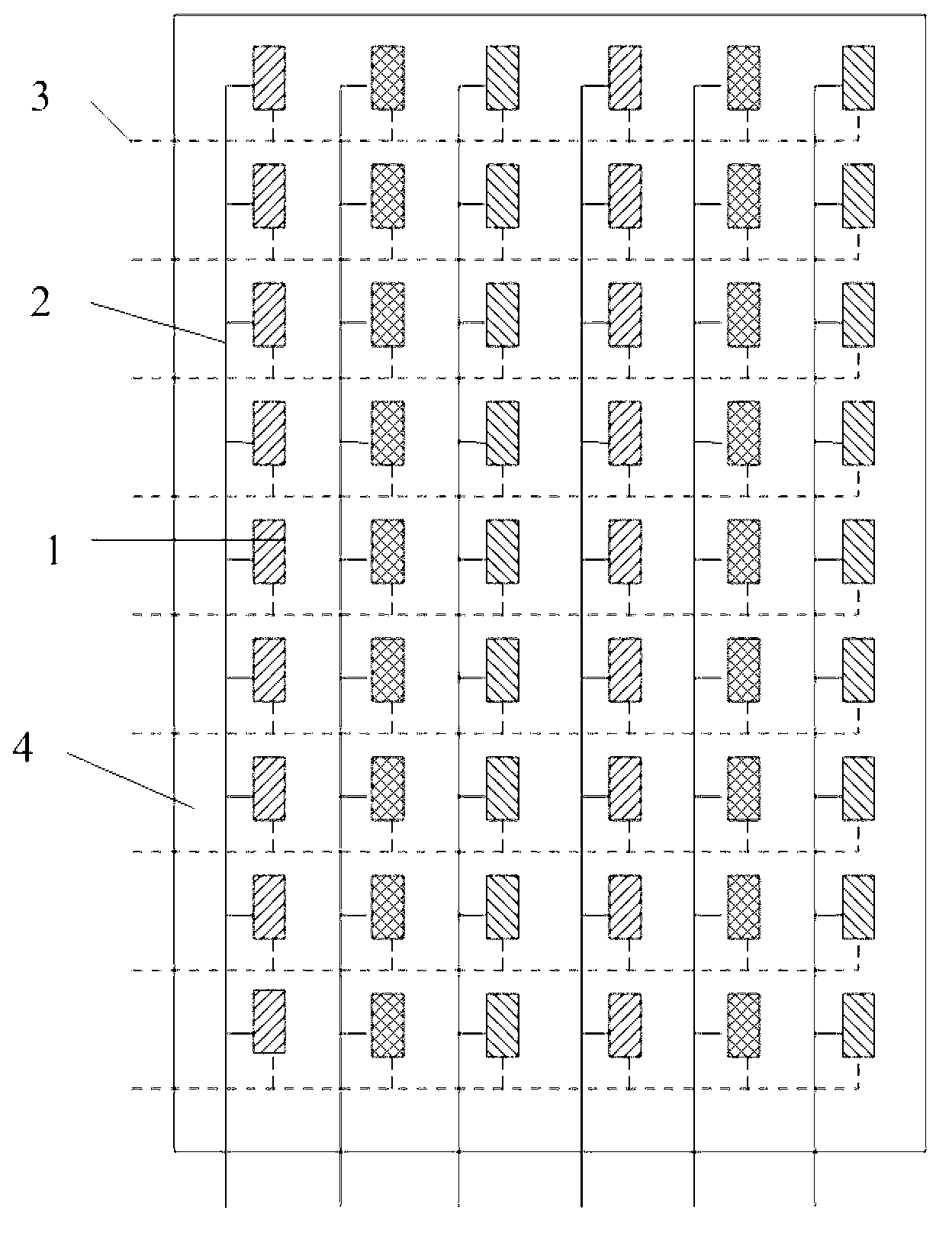
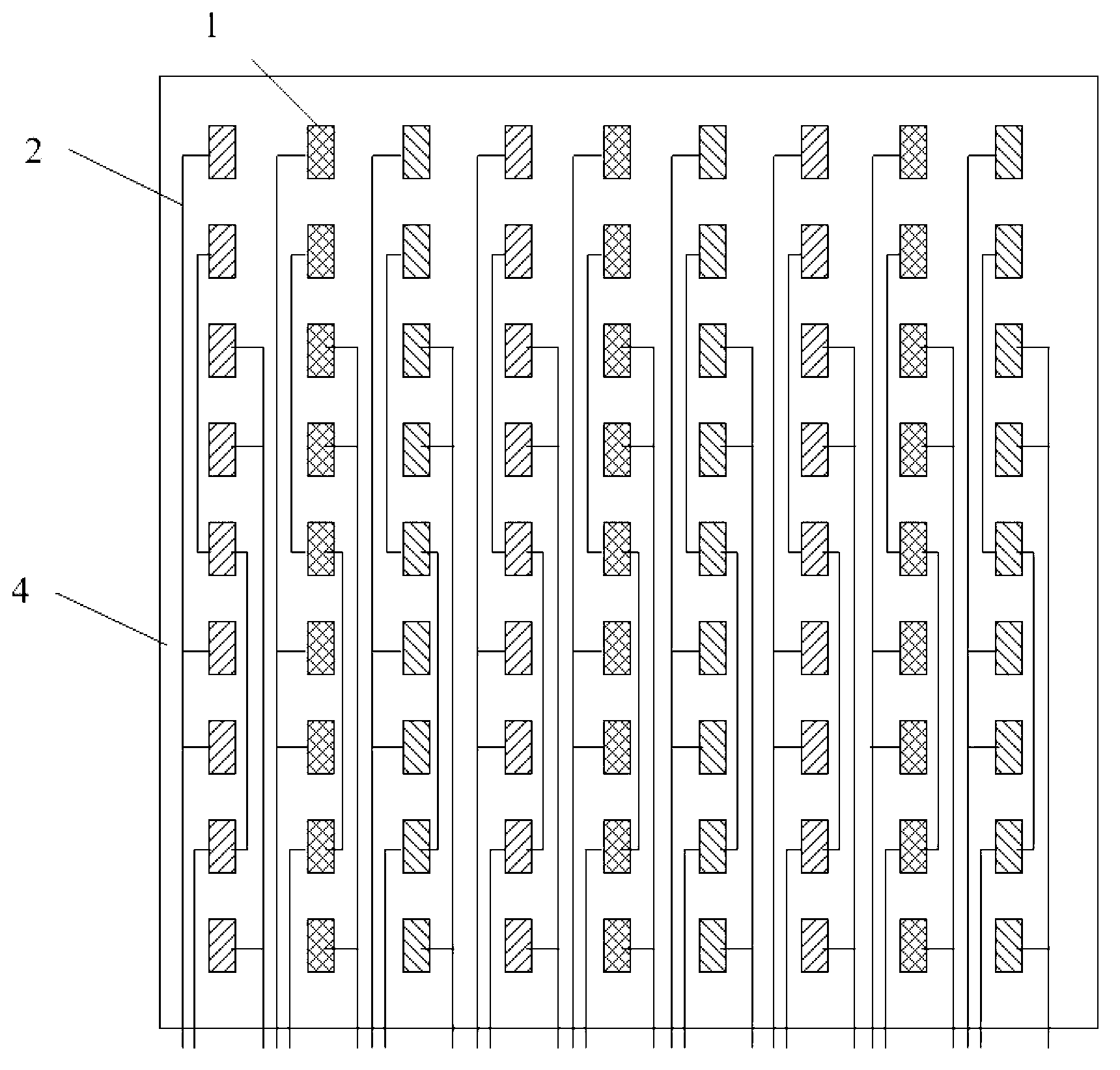
[0039] An OLED pixel structure, including a plurality of gate lines and data lines for driving OLED pixel units, the plurality of OLED pixel units are arranged in a matrix, and the OLED pixel units are scanned simultaneously by L rows, and are The OLED pixel units in every L rows scanned at the same time are set as a pixel block, where L≥3.
[0040] Wherein, a plurality of the OLED pixel units are arranged in an M*N (row*column) matrix, each of the OLED pixel units includes a plurality of color sub-pixel units, and each sub-pixel unit is arranged circularly in columns according to the color , the number of data lines is LN, and each L data line is respectively connected to the sub-pixel units in different rows of the same column; the number of gate lines is (2 / 3)M, and each gate line is connected to At least the sub-pixel units in adjacent rows in the same column are connected.
[0041] In this example, if Figure 3-5 As shown, L is preferably three, that is, the pixel units...
Embodiment 2
[0055] The difference between this embodiment and Embodiment 1 is that each pixel unit in this embodiment includes sub-pixel units of four colors, and the four colors are red, green, blue, and white respectively.
[0056] In this embodiment, the connection mode of the gate line and the data line in the OLED pixel structure and the output sequence of the image data in the timing control unit are similar to those in the first embodiment. Since the pixel unit includes sub-pixel units of four colors, specifically, the connection between the data line and the gate line in the pixel structure is as follows: Figure 9 Shown; the input sequence of the image data in the timing control unit is as follows Figure 10 As shown, the output sequence of the image data is as follows Figure 11 shown.
Embodiment 3
[0058]The difference between this embodiment and Embodiments 1 and 2 is that the connection mode of the gate lines in each pixel block in this embodiment is the same as that of the gate lines in the prior art, that is, each of the pixel blocks Three gate lines 3 are arranged in the pixel block, and each gate line is connected to a row of sub-pixel units, such as Figure 12 shown.
[0059] In Embodiments 1-3, the organic light-emitting diode pixel structure adopts a three-row scanning method during scanning, and three rows of sub-pixel units belonging to the same pixel block are turned on at the same time, and the image data of the three rows of sub-pixel units are simultaneously refreshed ; Cooperate with the image data processing method of the corresponding timing control unit for data processing, which can meet the image data arrangement requirements of this pixel structure. Since the row scan frequency is reduced to one-third of the row scan frequency in the prior art, the...
PUM
 Abstract
Description
Claims
Application Information


