Graphical circuit structure, manufacturing method thereof and application thereof
A circuit structure and graphic technology, applied in the direction of electrical digital data processing, instruments, data processing input/output process, etc., to achieve the effects of easy large-scale implementation, low cost, and improved product performance
- Summary
- Abstract
- Description
- Claims
- Application Information
AI Technical Summary
Problems solved by technology
Method used
Image
Examples
preparation example Construction
[0034] As an aspect of the present invention, the preparation method of the patterned circuit structure includes:
[0035] (1) forming a transparent conductive material layer at least in the first set area on the surface of the substrate;
[0036] (2) forming an insulating material layer in a second set area on the surface of the substrate;
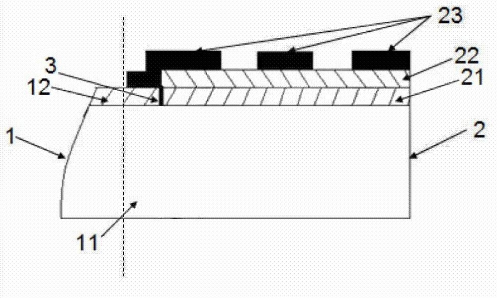
[0037] (3) Forming a circuit routing structure on the surface of the insulating material layer, and electrically connecting the circuit routing structure to the transparent conductive material layer, preferably, electrically connecting the circuit routing structure to the edge of the transparent conductive material layer.
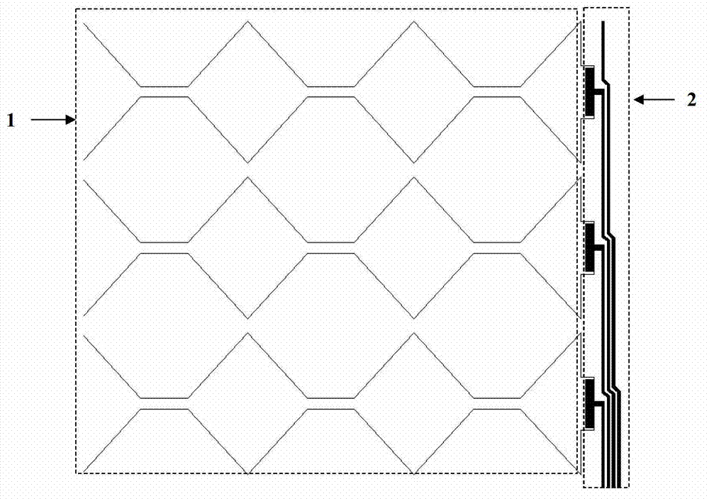
[0038] In some specific application schemes, the second set area is arranged around the first set area, and at least the inner edge of the insulating material layer is joined to the outer edge of the transparent conductive material layer.
[0039] As one of the more preferred embodiments, the preparation method may al...
Embodiment 1
[0058] This embodiment firstly provides a transparent conductive film of carbon nanotubes with a 4.3-inch rhombic pattern covered on a substrate as a transparent conductive electrode. Continuous etching is carried out around the visible area, and the etching depth should reach the surface of the substrate or go deep into the interior of the substrate, so as to completely isolate the transparent conductive electrode in the visible area from the non-visible area. Through precise positioning, use flexographic printing to print epoxy resin outside the diamond pattern frame (that is, the visible area) and in the area where the silver line is printed (that is, the non-visible area), and dry it with hot air in an oven at 80°C. Screen printing prints silver paste on the surface of the cured epoxy resin to form circuit traces connected to the edge of the electrode material, and dries with hot air at 130°C to obtain a sensor for capacitive touch screens.
Embodiment 2
[0060] This embodiment firstly provides a transparent conductive film of silver nanowires with a 4.3-inch diamond pattern covered on a substrate as a transparent conductive electrode. Continuous etching is carried out around the visible area, and the etching depth should reach the surface of the substrate or go deep into the interior of the substrate, so as to completely isolate the transparent conductive electrode in the visible area from the non-visible area. Through precise positioning, use flexographic printing method to print silicone resin outside the rhombus pattern frame (that is, the visible area) and in the area where the silver line is printed (that is, the non-visible area), and dry it with hot air in an oven at 120 ° C. Screen printing prints silver paste on the surface of the cured silicone resin to form circuit traces connected to the edge of the electrode material, and dries with hot air at 130°C to obtain a sensor for capacitive touch screens.
PUM
 Abstract
Description
Claims
Application Information

