Organic electroluminescent device and production method thereof

An electroluminescence device and electroluminescence technology, which are applied in the fields of electric solid state devices, chemical instruments and methods, semiconductor/solid state device manufacturing, etc., and can solve the problems of low contrast and inability to see the content clearly.

Inactive Publication Date: 2013-06-05
OCEANS KING LIGHTING SCI&TECH CO LTD +1
View PDF3 Cites 6 Cited by
  • Summary
  • Abstract
  • Description
  • Claims
  • Application Information

AI Technical Summary

Problems solved by technology

[0004] OLEDs generally use metal cathode materials with high reflectivity, but high reflectivity cathodes make organic electr...

Method used


Image

  • Organic electroluminescent device and production method thereof
  • Organic electroluminescent device and production method thereof
  • Organic electroluminescent device and production method thereof

Examples


preparation example Construction

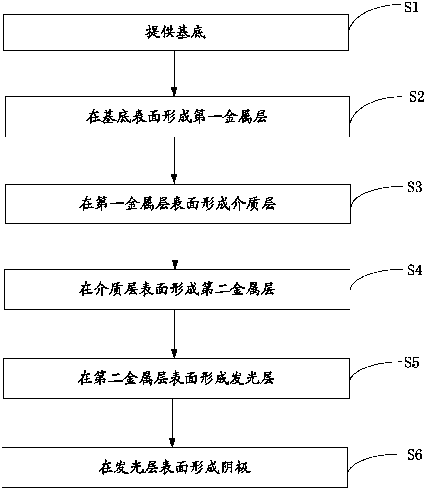
[0032] see figure 2 , the preparation method of the organic electroluminescent device of an embodiment, comprises the following steps:

[0033] Step S1 , providing a substrate 10 .

[0034] In this embodiment, the substrate is silicon wafer, glass or polymer film material. Substrates are cleaned prior to use. First, put the substrate in deionized water containing detergent for ultrasonic cleaning. After cleaning, it is treated with isopropanol and acetone in ultrasonic for 20 minutes, and then dried with nitrogen to obtain a clean substrate.

[0035] Step S2, forming a first metal layer 21 on the substrate surface 10, the material of the first metal layer 21 is aluminum (Al), silver (Ag), gold (Au), aluminum-silver alloy (Al-Ag) or magnesium-silver alloy ( Mg-Ag). The thickness of the first metal layer 21 is 80nm˜150nm.

[0036] In this embodiment, the first metal layer 21 is formed by evaporation in a vacuum coating system.

[0037]Step S3 , forming a dielectric layer ...

Embodiment 1

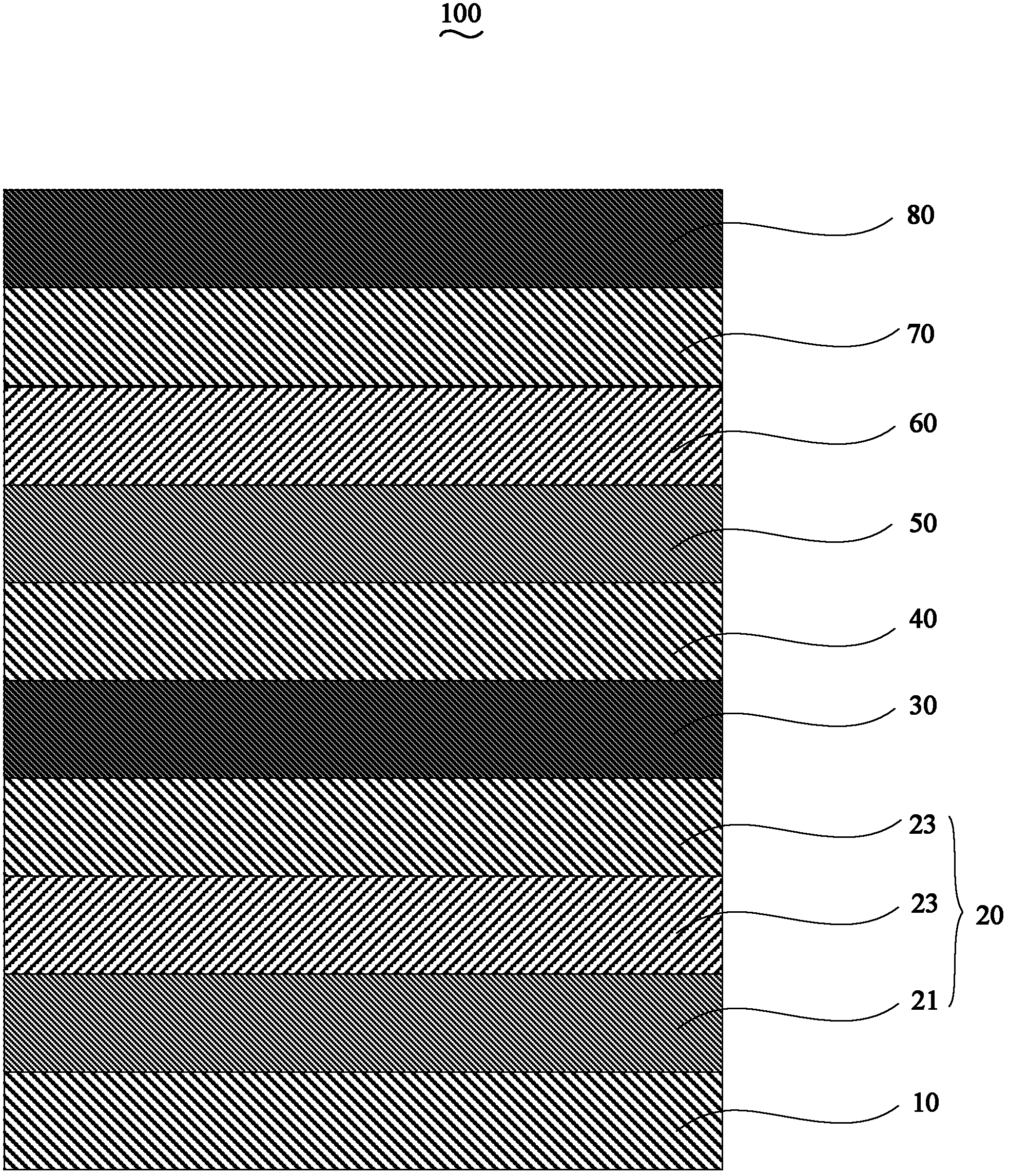
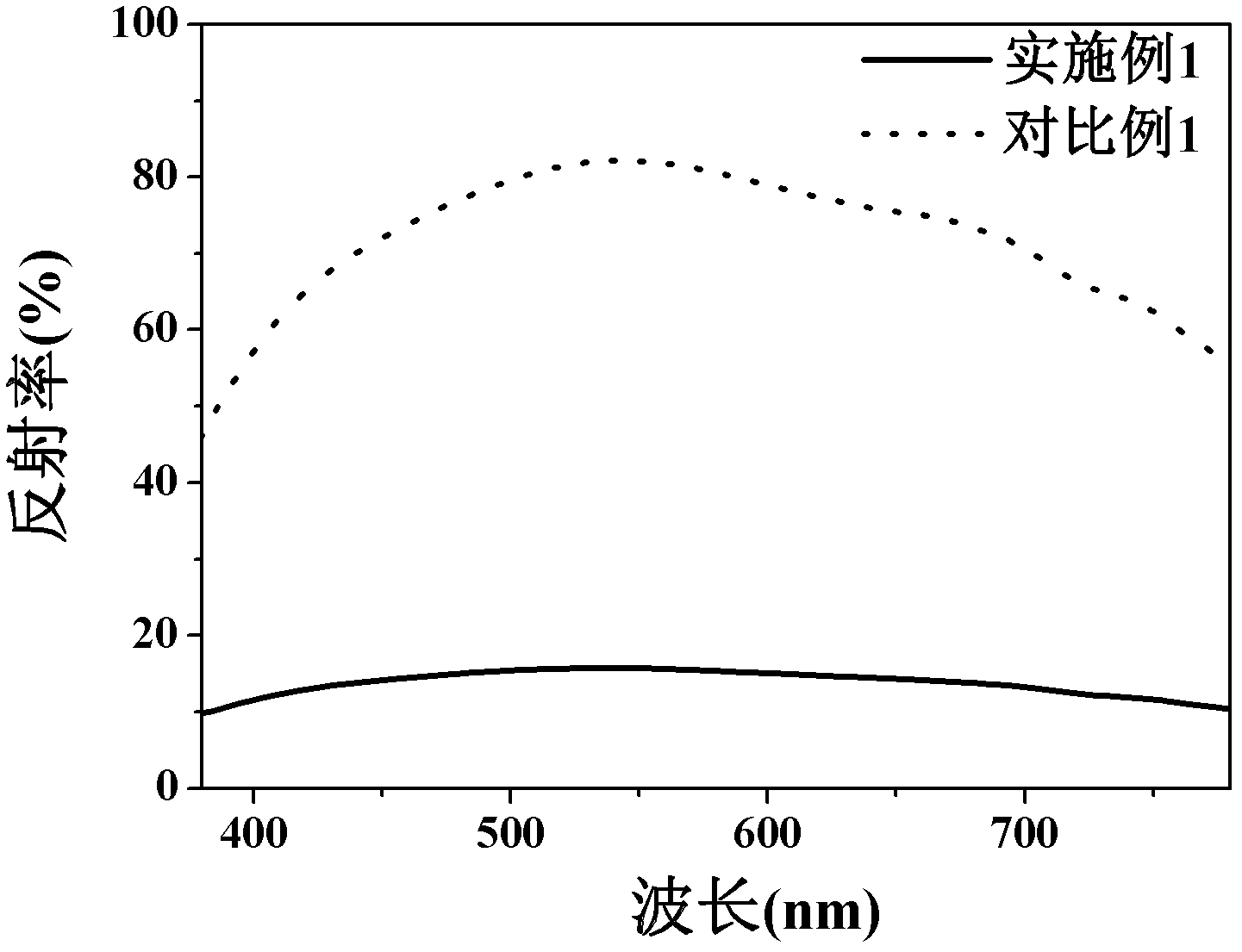
[0050] The structure of the organic electroluminescent device of this embodiment 1: substrate / Ag / IZO / Ag / m-MTDATA / NPB / FIrPic:CBP / Alq 3 / LiF / Ag.

[0051] The preparation process of the organic electroluminescent device of this embodiment 1 is as follows:

[0052] Place the glass substrate in deionized water containing detergent for ultrasonic cleaning. After cleaning, treat it with isopropanol and acetone in ultrasonic for 20 minutes, and then dry it with nitrogen. In the vacuum evaporation system, metal Ag with a thickness of 100 nm is deposited on the surface of the substrate as the first metal layer, and then transferred to the magnetron sputtering system to prepare indium-doped zinc oxide with a thickness of 80 nm on the first metal layer (IZO) thin film is used as a dielectric layer, and then transferred to a thermal evaporation system, and a metal Ag with a thickness of 8 nm is evaporated on the dielectric layer as a second metal layer to prepare an anode. The anode was ...

Embodiment 2

[0055] The structure of the organic electroluminescent device in Example 2: substrate / Al / ITO / Al / m-MTDATA / NPB / FIrPic:CBP / Alq 3 / LiF / Al / Ag.

[0056] In the anode structure prepared in Example 2, the first metal layer is an Al layer with a thickness of 80nm, the dielectric layer is an indium-doped tin oxide (ITO) film with a thickness of 60nm, and the second metal layer is an Al layer with a thickness of 6nm . Referring to Example 1, after the anode is treated, continue to vapor-deposit a hole injection layer, a hole transport layer, a light-emitting layer, an electron transport layer, and an electron injection layer on the surface in sequence, and the thicknesses are 30nm, 30nm, 15nm, and 60nm respectively. , 1nm, and the subsequent cathode is a double-layer structure composed of Al(1nm) / Ag(20nm).


PUM

PropertyMeasurementUnit
Thicknessaaaaaaaaaa
Thicknessaaaaaaaaaa
Thicknessaaaaaaaaaa

Abstract

An organic electroluminescent device comprises a substrate, an anode, a luminous layer and a cathode which are sequentially arranged in a laminating mode. The anode comprises a first metal layer, a dielectric layer and a second metal layer which are sequentially arranged on the substrate in a laminating mode, wherein the first metal layer is made of aluminum, silver, gold, aluminum-silver alloy, or magnesium- silver alloy and the thickness of the first metal layer is from 80 to 150 nm; the dielectric layer is made of transparent conductive oxide materials and the thickness of the dielectric layer is from 60 to 100 nm; and the second metal layer is made of aluminum, silver or gold and the thickness of the second metal layer is from 6 to 12 nm. The organic electroluminescent device has the advantage of being low in reflectivity. The invention also provides a production method of the organic electroluminescent device.

Description

【Technical field】 [0001] The invention relates to an organic electroluminescence device and a preparation method thereof. 【Background technique】 [0002] Organic Light Emission Diode (Organic Light Emission Diode) or organic electroluminescent device, referred to as OLED, has the characteristics of high brightness, wide range of material selection, low driving voltage, fully cured active light, etc., and has high definition, wide viewing angle, and It can smoothly display the advantages of high-speed response of animation, and OLED can be made into a flexible structure, which can be folded and bent. It is a flat panel display technology and planar light source with great potential, which conforms to the development trend of mobile communication and information display in the information age, and The requirement of green lighting technology has been a very hot research field in the last ten years. [0003] Organic electroluminescent diodes have a sandwich-like structure, wit...

Claims


Application Information

Patent Timeline
IPC IPC(8): H01L51/52H01L51/54H01L51/56C09K11/06
Inventor 周明杰王平冯小明张振华
Owner OCEANS KING LIGHTING SCI&TECH CO LTD
Why Eureka
Try Eureka