Active pixel of complementary metal oxide semiconductor (CMOS) image sensor and CMOS image sensor

An image sensor and pixel technology, applied in the field of image sensors, can solve the problem that linear sensors are not easy to collect physical information, and achieve the effects of improving photosensitive sensitivity, high photoelectric conversion gain, and high sensitivity

Active Publication Date: 2013-06-05
BEIJING SUPERPIX MICRO TECHNOLOGY CO LTD
View PDF6 Cites 7 Cited by
  • Summary
  • Abstract
  • Description
  • Claims
  • Application Information

AI Technical Summary

Problems solved by technology

[0005] The technical problem to be solved by the present invention is to provide an active pixel of a CMOS image sensor and a CMOS image sensor, which can ensure the quality of the output image, thereby solving the problem that the linear sensor is difficult to collect physical information in a low-light environment

Method used


Image

  • Active pixel of complementary metal oxide semiconductor (CMOS) image sensor and CMOS image sensor
  • Active pixel of complementary metal oxide semiconductor (CMOS) image sensor and CMOS image sensor
  • Active pixel of complementary metal oxide semiconductor (CMOS) image sensor and CMOS image sensor

Examples


Embodiment Construction

[0017] The following describes the technical solutions in the embodiments of the present invention clearly and completely. Obviously, the described embodiments are only a part of the embodiments of the present invention, rather than all the embodiments. Based on the embodiments of the present invention, all other embodiments obtained by those of ordinary skill in the art without creative work shall fall within the protection scope of the present invention.

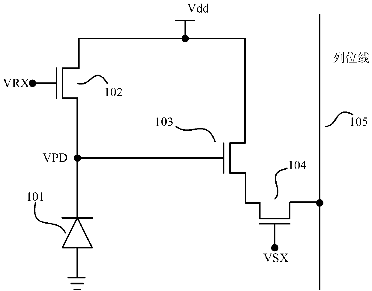
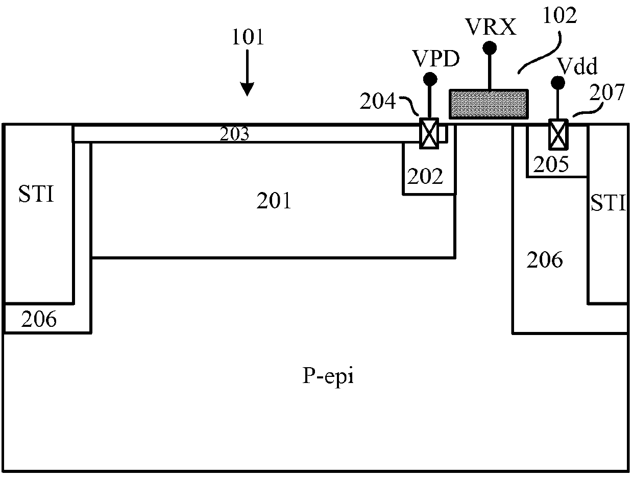
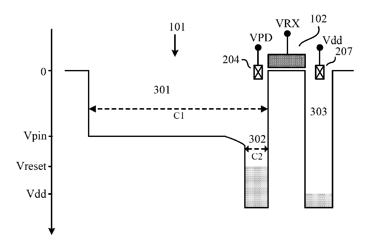
[0018] The embodiment of the present invention provides an active pixel, such as figure 2 As shown, the active pixel includes at least a photosensitive element placed in a semiconductor substrate, a reset transistor and a source follower transistor connected to the photosensitive element, a switch transistor and a column bit line. The photosensitive element has two photosensitive regions: low-dose impurity ions The implantation area and the high-dose impurity ion implantation area near the reset transistor.

[0019] The low-do...


PUM


Abstract

The invention discloses an active pixel of a complementary metal oxide semiconductor (CMOS) image sensor. The active pixel at least comprises a photosensitive component which is placed inside a semi-conductor substrate, a reset transistor and a source following transistor which are connected with the photosensitive component, a switch transistor, and a row positioning line. The pixel photosensitive component of the image sensor comprises two photosensitive regions, namely a low dose foreign ion injection region, and a high dose foreign ion injection region near the reset transistor. When in low illumination, photo-electricity charge generated in the photosensitive component is only collected in the high dose foreign ion injection region, grain of photo-electricity transition is high, and sensitivity of the sensor is high. When in high illumination, photo-electricity charge generated in the photosensitive component is collected in the whole photosensitive component. Therefore, the active pixel can effectively improve the luminous sensitivity of the image sensor in the low illumination, and the sensor collects more real object detail information when in the low illumination.

Description

Technical field [0001] The invention relates to an image sensor, in particular to an active pixel of a CMOS image sensor and a CMOS image sensor. Background technique [0002] Image sensors have been widely used in digital cameras, mobile phones, medical equipment, automobiles and other applications. Especially the rapid development of manufacturing CMOS (Complementary Metal Oxide Semiconductor) image sensor technology has made people have higher requirements for the output image quality of the image sensor. [0003] In the prior art, CMOS image sensors generally adopt a pixel structure with linear photoelectric response function. Such as figure 1 As shown, the CMOS image sensor uses a three-transistor active pixel, which is also called a 3T active pixel in the art. The components of the 3T active pixel include: a photodiode 101, a reset transistor 102, a source follower transistor 103, and a switching transistor 104, and the column bit line 105; one end VPD of the photodiode 101...

Claims


Application Information

Patent Timeline
Patent Type & Authority Applications(China)
IPC IPC(8): H04N5/374H04N5/359
Inventor 郭同辉唐冕陈杰刘志碧旷章曲
Owner BEIJING SUPERPIX MICRO TECHNOLOGY CO LTD
Why Eureka
Try Eureka