Image sensor active pixel and image sensor with variable conversion gain

An image sensor and conversion gain technology, applied in the field of image sensors, can solve the problems of reducing the output image quality of the sensor, difficult to collect, etc., and achieve the effects of improving image quality, low photoelectric conversion gain, and high photoelectric conversion gain.

Active Publication Date: 2016-08-31
BEIJING SUPERPIX MICRO TECHNOLOGY CO LTD
View PDF4 Cites 0 Cited by
  • Summary
  • Abstract
  • Description
  • Claims
  • Application Information

AI Technical Summary

Problems solved by technology

In the outdoor environment, the linear sensor is not easy to collect the physical information of the high lighting environment, thus reducing the output image quality of the sensor

Method used


Image

  • Image sensor active pixel and image sensor with variable conversion gain
  • Image sensor active pixel and image sensor with variable conversion gain
  • Image sensor active pixel and image sensor with variable conversion gain

Examples


Embodiment Construction

[0024] The following clearly and completely describes the technical solutions in the embodiments of the present invention. Obviously, the described embodiments are only some of the embodiments of the present invention, but not all of them. Based on the embodiments of the present invention, all other embodiments obtained by persons of ordinary skill in the art without making creative efforts belong to the protection scope of the present invention. In addition, well-known structures and operations are not shown or described in detail in order to clearly describe the various embodiments of the present invention.

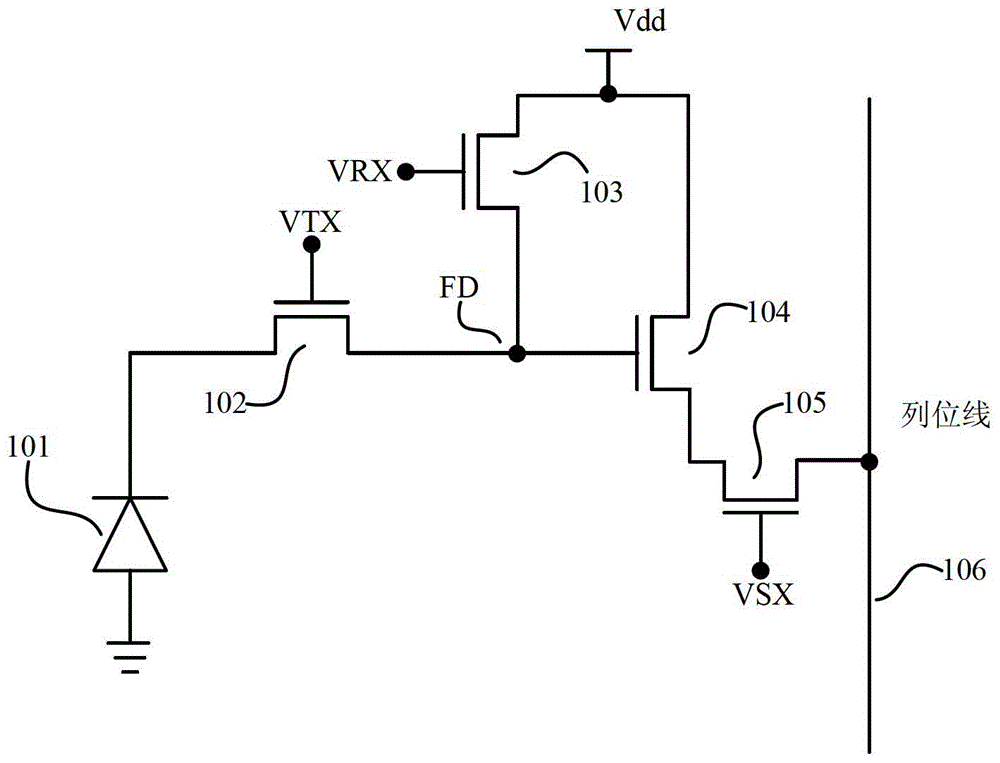
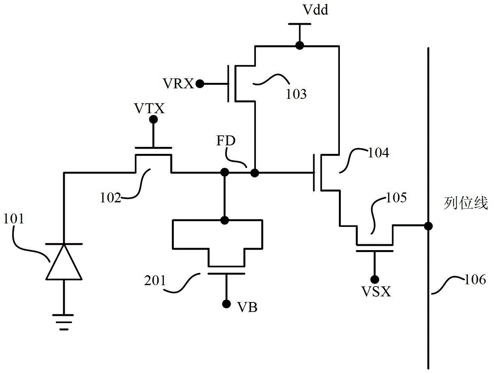
[0025] The embodiment of the present invention introduces a special pixel structure to the floating active area to form a new 4T active pixel, figure 2 Shown is the circuit diagram of the active pixel structure, from figure 2 It can be seen from the figure that the 4T active pixel is basically the same as the current 4T active pixel. The gate terminal VB of the capa...


PUM


Abstract

The invention discloses an imaging sensor active pixel and an imaging sensor with variable conversion gain and belongs to the field of the imaging sensor. The active pixel comprises a photosensitive element which is arranged in a semiconductor base body, a charge transfer transistor which connected with the photosensitive element, a reset transistor, a source following transistor, a row choosing transistor, a transistor capacitor and a floating active area, wherein a source drain electrode of the transistor capacitor is connected with the floating active area, and a grid electrode of the transistor capacitor is connected with an external input voltage. In a low luminous environment, a gate-oxide layer capacitor portion of the transistor capacitor is not in line with a capacitor of the floating active area. In a high luminous environment, a great quantity of photoelectricity charges enable potential of the floating active area to be reduced, so that the gate-oxide layer capacitor portion of the transistor capacitor is enabled to be in line with the capacitor of the floating active area. Therefore, the active pixel effectively delays saturated time of the imaging sensor in the high luminous environment, and the sensor collects more real object detail information in the high luminous environment.

Description

technical field [0001] The invention relates to the field of image sensors, in particular to an image sensor active pixel with variable conversion gain and the image sensor. Background technique [0002] Image sensors have been widely used in digital cameras, mobile phones, medical devices, automobiles and other applications. In particular, the rapid development of CMOS (Complementary Metal Oxide Semiconductor) image sensor technology has made people have higher requirements for the output image quality of image sensors. [0003] In the prior art, a CMOS image sensor generally adopts a pixel structure with a linear photoelectric response function. like figure 1 As shown, it is an active pixel using four transistors of a CMOS image sensor, which is also called a 4T active pixel in the field. The components of a 4T active pixel include: a photodiode 101, a charge transfer transistor 102, a reset transistor 103, a source follower transistor 104, a row selection transistor 10...

Claims


Application Information

Patent Timeline
Patent Type & Authority Patents(China)
IPC IPC(8): H04N5/374H04N5/359
Inventor 郭同辉唐冕陈杰刘志碧旷章曲
Owner BEIJING SUPERPIX MICRO TECHNOLOGY CO LTD
Why Eureka
Try Eureka