Bus interface patch board and data transmission system
A technology of bus interface and adapter board, which is applied in the field of data transmission system based on bus interface, can solve the problems of low test efficiency and stability, and achieve the effects of improving efficiency, ensuring stability and accuracy, and being convenient to use
- Summary
- Abstract
- Description
- Claims
- Application Information
AI Technical Summary
Problems solved by technology
Method used
Image

Examples
Embodiment 1
[0034] refer to figure 1 , a structural diagram of a bus interface adapter board described in Embodiment 1 of the present invention is given.
[0035] Wherein, the bus interface adapter board 1 includes a bus interface connector J1 and a USB interface J2.
[0036] In this embodiment, the bus interface is an interface of the PCI-E bus, and the bus interface connector J1 in the bus interface adapter board 1 can adopt various devices of the PCI-E bus.
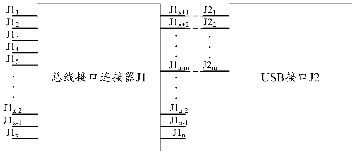
[0037] Wherein, the bus interface connector J1 includes n connecting wires, and one end of the n connecting wires is respectively used to connect to the corresponding n pins in the bus interface, where n is a positive integer;
[0038] The USB interface J2 includes m data lines, and one end of the m data lines is respectively used to connect to corresponding m data lines in a general-purpose USB device, wherein m is a positive integer.
[0039] The other end of the m data lines in the USB interface J2 is respectively connected t...
Embodiment 2
[0054] refer to figure 2 , which provides a structural diagram of the bus interface adapter board described in Embodiment 2 of the present invention.
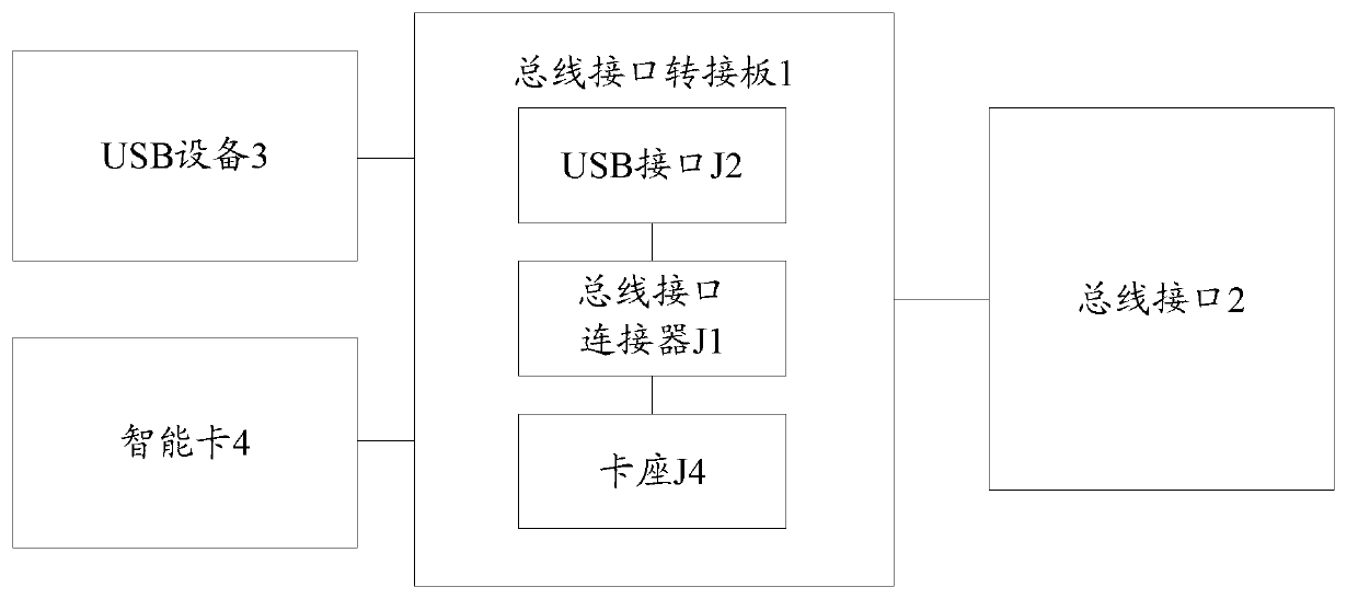
[0055] refer to image 3 , which shows the structure diagram of the data transmission system based on the bus interface described in the second embodiment of the present invention. For the convenience of description, in this embodiment, the figure 2 and image 3 Combine instructions. image 3 The data transmission system based on the bus interface includes figure 2 The bus interface adapter board also includes a USB device and a bus interface.
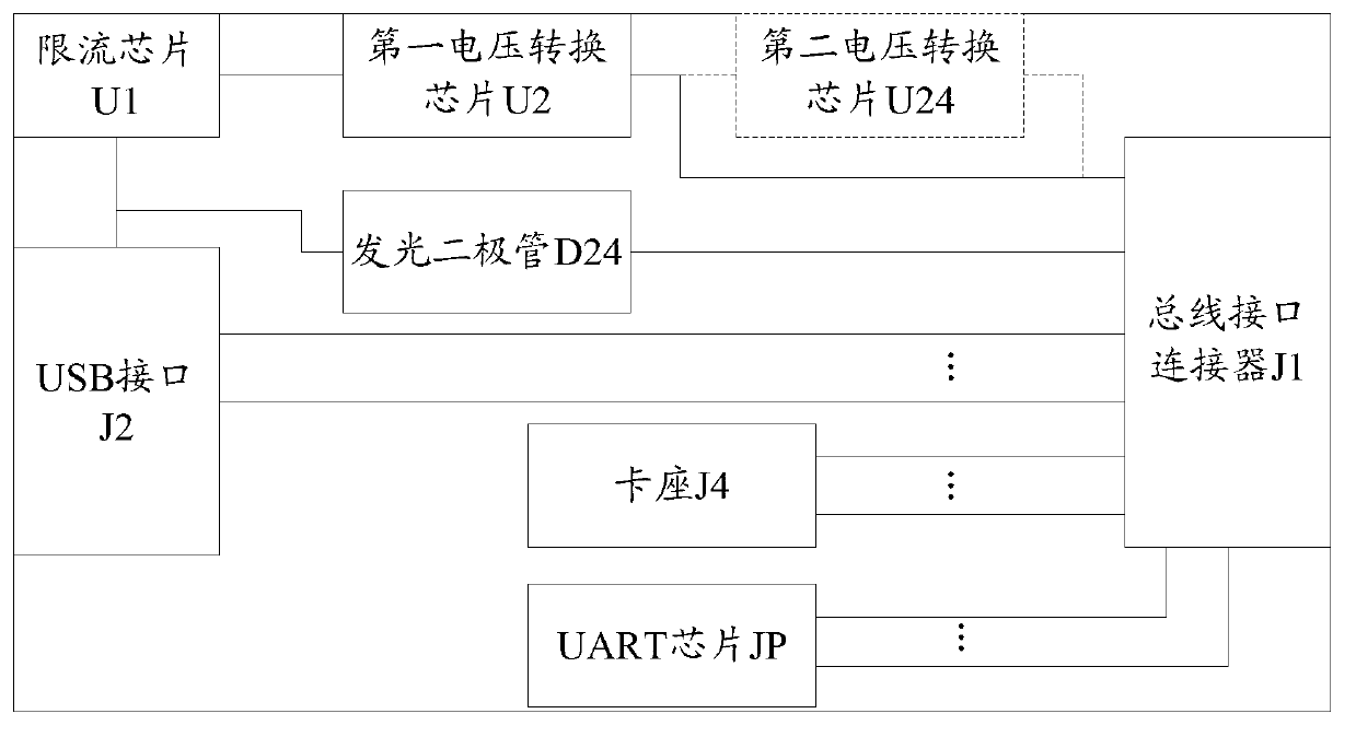
[0056] In this embodiment, the bus interface adapter board 1 includes: a bus interface connector J1 and a USB interface J2.
[0057] Wherein, the bus interface connector J1 includes n connection wires, and one end of the n connection wires is respectively used to connect to the corresponding n pins in the bus interface 2, wherein n is a positive integer.
[0058] The USB inter...
Embodiment 3
[0103] In this embodiment, the bus interface adopts MINI PCI-E in order to discuss an implementation of the line interface connector J1 in detail. The bus interface connector J1 is a MINI PCI-E connector J1, wherein the MINIPCI-E is a 52-pin device, and each pin of the MINI PCI-E can be called a pin. Then n=52 in MINI PCI-E connector J1.
[0104] refer to Figure 4 , a schematic diagram of the pins of the MINI PCI-E connector described in Embodiment 3 of the present invention is given.
[0105] MINI PCI-E connector J1, when n=52, the connection line J1 of MINI PCI-E connector J1 l ~J1 n Corresponding respectively Figure 4 The connection lines identified by 1 to 52 in . In specific implementation, due to different specific requirements, the MINI PCI-E connector J1 may not only include n connecting wires, such as Figure 4 The two connecting wires 53 and 54 are also included, and the two connecting wires can be grounded.
[0106] Wherein, the connection line correspondin...
PUM
 Abstract
Description
Claims
Application Information
 - R&D
- Intellectual Property
- Life Sciences
- Materials
- Tech Scout
- Unparalleled Data Quality
- Higher Quality Content
- 60% Fewer Hallucinations
Browse by: Latest US Patents, China's latest patents, Technical Efficacy Thesaurus, Application Domain, Technology Topic, Popular Technical Reports.
© 2025 PatSnap. All rights reserved.Legal|Privacy policy|Modern Slavery Act Transparency Statement|Sitemap|About US| Contact US: help@patsnap.com