

Data driver, display panel driving device, and display device
A data driver and output circuit technology, applied in the direction of instruments, semiconductor devices, static indicators, etc., can solve problems such as operation failure
- Summary
- Abstract
- Description
- Claims
- Application Information
AI Technical Summary
Problems solved by technology
Method used
Image

Examples
no. 1 example
[0049] The configuration of the display device according to the first embodiment of the present invention will be described below. Figure 8 is a block diagram showing an example of the configuration of the display device according to the first embodiment of the present invention. The display device 50 is a thin film transistor (TFT) type liquid crystal display device. The display device 50 includes a display unit (liquid crystal display panel) 60 , a gate driver 70 , a plurality of data drivers 1 , and a timing controller 52 .
[0050] The display unit (liquid crystal display panel) 60 is a liquid crystal display (LCD) module. The display unit 60 includes a plurality of gate lines 67 , a plurality of data lines 68 and a plurality of pixels 61 . The gate lines 67 extend in the X direction. The data line 68 extends in the Y direction. The pixels 61 are arranged in a matrix corresponding to points where the gate lines 67 and the data lines 68 intersect. The pixel 61 include...
no. 2 example
[0091] The configuration of a display device and a data driver according to a second embodiment of the present invention will be described below. In this embodiment, the delay circuit in the data driver is different from that in the first embodiment. The following description focuses primarily on this difference.
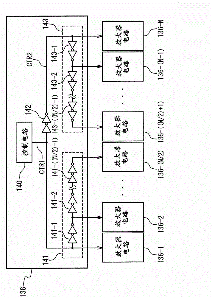
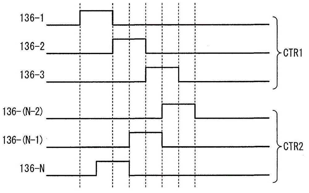
[0092] Figure 15 is a block diagram showing an example of the configuration of the data driver of the display device according to the second embodiment of the present invention. In the data driver 1 according to the first embodiment, the delay circuit is broadly divided into three sections (delay circuits 6 , 7 and 8 ) based on the load of the signal line 12 . On the other hand, in the data driver 1a according to the second embodiment, the delay time of the delay circuit is gradually changed according to the gradual change in the length of the signal line 12 of the amplifier circuit 3 . This will be described in detail below.
[0093] The amplifier circuit driv...
no. 3 example
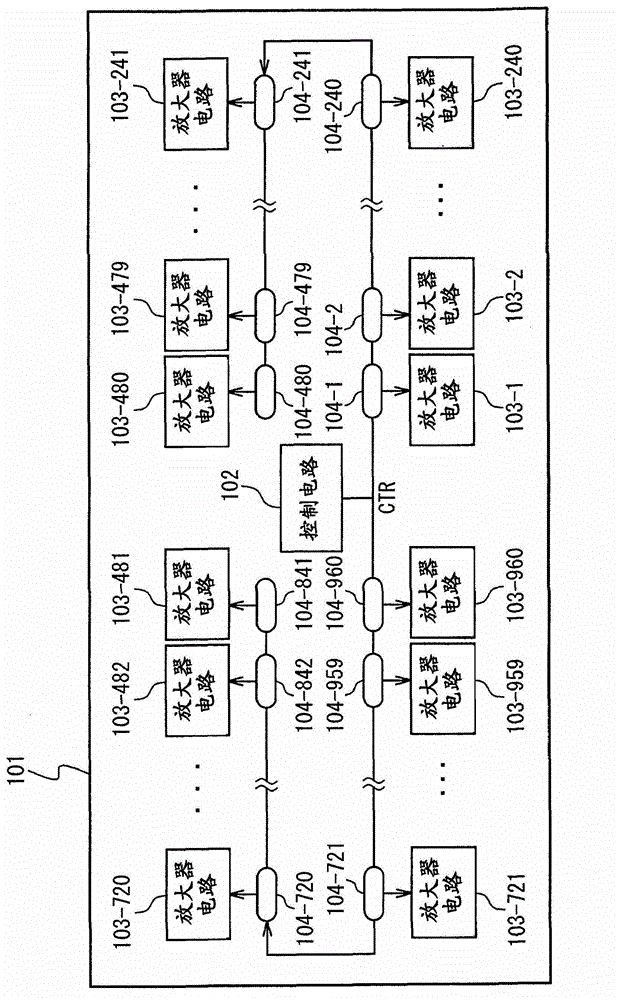
[0106] The configuration of a display device and a data driver according to a third embodiment of the present invention will be described below. In this embodiment, the delay circuit of the data driver is different from that in the first embodiment. The following description will mainly focus on this difference.
[0107] Figure 16 is a block diagram showing an example of a configuration of a data driver of a display device according to a third embodiment of the present invention. In the data driver 1 according to the first embodiment, the delay circuits are broadly divided into three groups based on the load of the signal line 12 in which the delay time gradually decreases (from large delay to medium delay, and to small delay). On the other hand, the data driver 1b according to the third embodiment further includes a delay circuit after a specific delay circuit group so as to increase the delay time again (after a small delay to an increasing delay or a large delay). This ...
PUM
 Abstract
Description
Claims
Application Information