Printed circuit board (PCB) and processing method
A technology of PCB board and processing method, which is applied in the field of electronics, can solve the problems of high cost and achieve the effects of low cost, simple process and short processing cycle
- Summary
- Abstract
- Description
- Claims
- Application Information
AI Technical Summary
Problems solved by technology
Method used
Image

Examples
Embodiment Construction
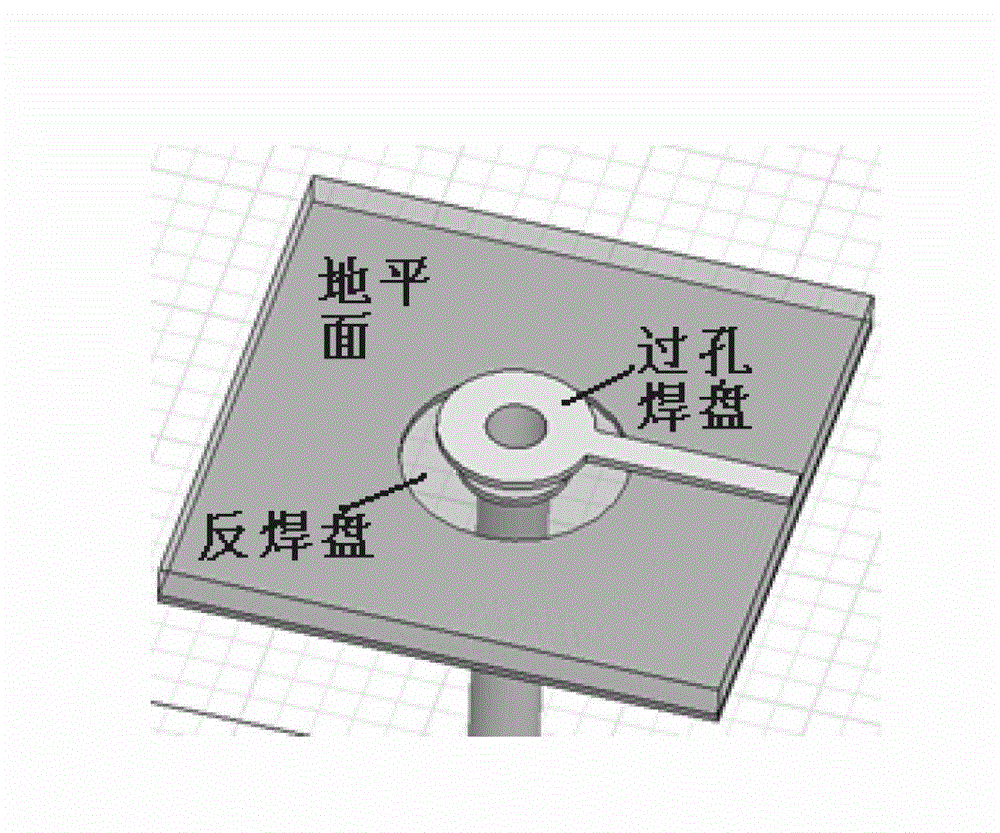
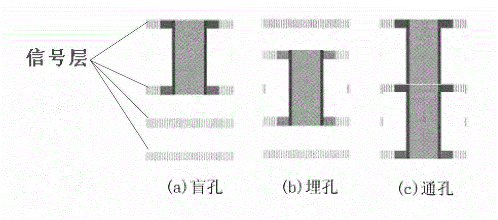
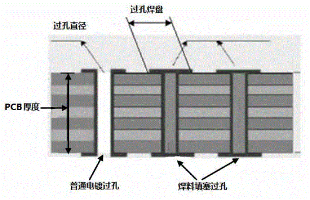
[0018] In order to achieve the purpose of the present invention, the present invention provides a PCB board processing method, the general concept of which is to fill the via holes of the PCB board with low-cost and easily obtained solder to improve the electrical characteristics of the via holes. In a preferred solution, the present invention injects liquid filling solder into the through holes of the PCB board during the processing of the PCB, and then cools the PCB board so that the liquid filling solder is cooled to non-liquid filling solder, Finally, solder is filled in the via holes. Further, the solder filling can be realized by the method of reflow soldering or wave soldering. The invention can effectively improve the signal quality and the flow capacity of the via hole on the PCB, thereby improving the signal quality of the circuit on the PCB and the flow capacity of the system current.
[0019] In order to make the technical solution of the present invention clearer...
PUM
 Abstract
Description
Claims
Application Information