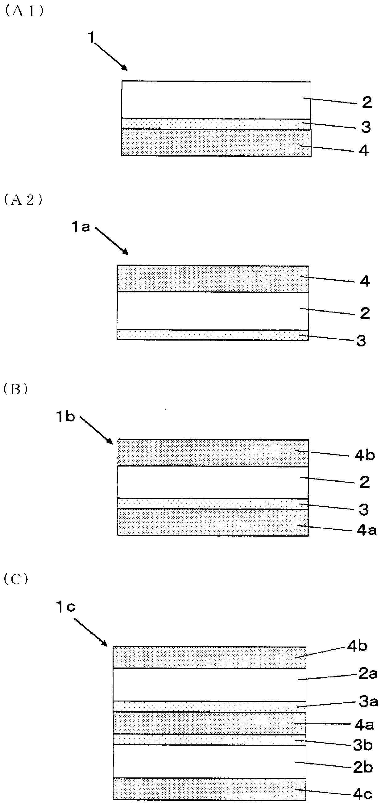
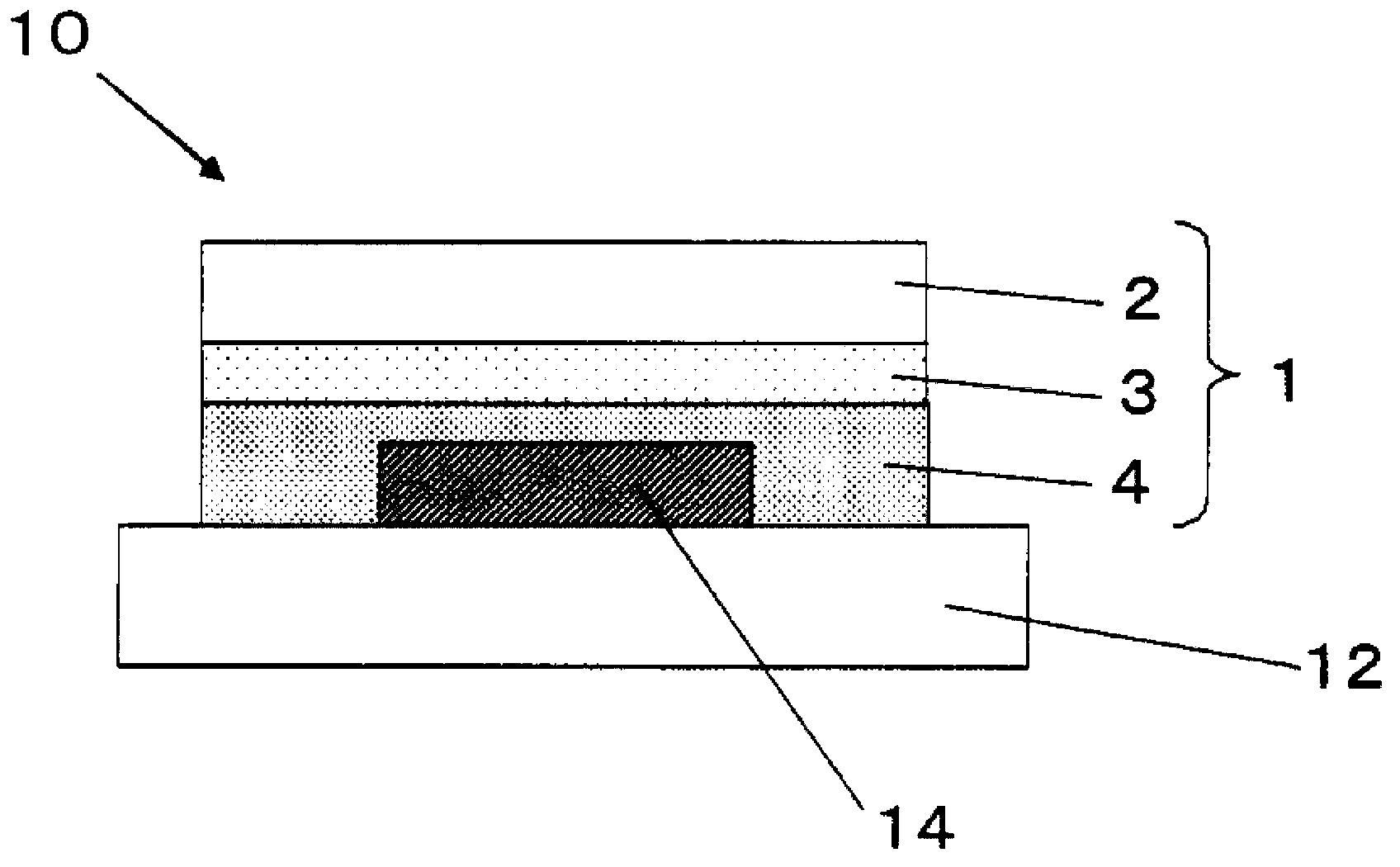
Adhesive sheet and electronic device
A technology of adhesive sheet and adhesive layer, applied in the direction of circuits, adhesives, electrical components, etc., can solve the problems of reduced performance of adhesive films, degradation of organic EL elements, degradation of adhesive layers, etc., and achieve good gas barrier effect
- Summary
- Abstract
- Description
- Claims
- Application Information
AI Technical Summary
Problems solved by technology
Method used
Image

Examples
preparation example Construction
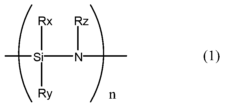
[0089] As a specific production method, for example, an organopolysilazane can be synthesized by reacting ammonia or a primary amine with a reaction product which is an unsubstituted or substituted halosilane represented by the following formula (9): The reaction product of a compound with a secondary amine. The secondary amines and primary amines to be used may be appropriately selected according to the structure of the target polysilazane compound.
[0090] [chemical formula 9]
[0091] R 1 4-m SiX m (9)
[0092] (In formula (9), m represents 2 or 3, X represents a halogen atom, R 1 Represents any substituent of the aforementioned Rx, Ry, Rz, Rx', Ry', and Rz'. )
[0093] In addition, in the present invention, a modified polysilazane can also be used as the polysilazane compound. Examples of modified polysilazanes include polymetallosilazanes containing metal atoms (the metal atoms can also form crosslinks), [(SiH 2 ) g (NH) h )] and [(SiH 2 ) i O] (wherein,...
Embodiment
[0222] Hereinafter, the present invention will be described in more detail with reference to examples. However, the present invention is not limited in any way by the following Examples.
[0223] Plasma ion implantation equipment used, XPS measurement equipment, film density measurement equipment using X-ray reflectivity method, bending test method, water vapor transmission rate measurement equipment and measurement conditions, water at the end of the adhesive layer The method of the vapor transmission test, the method of measuring the adhesive force, and the apparatus for measuring the visible light transmittance are as follows.
[0224] (Plasma ion implantation device)
[0225] RF power supply: manufactured by JEOL Ltd., model "RF" 56000
[0226] High-voltage pulse power supply: "PV-3-HSHV-0835" manufactured by Kurita Manufacturing Co., Ltd.
[0227] In addition, the plasma ion implantation apparatus used is an apparatus that implants ions using an external electric field...
preparation example 1)
[0282] A polysilazane compound is applied by spin coating on a polyethylene terephthalate film (manufactured by Mitsubishi Plastics Corporation, "PET38T-100", 38 μm thick, hereinafter referred to as "PET film") as a base material A, Heated at 120° C. for 1 minute to form a polysilazane layer containing perhydropolysilazane with a thickness of 60 nm on the PET film. Next, argon (Ar) was implanted with plasma ions on the surface of the perhydropolysilazane-containing layer using a plasma ion implantation apparatus to produce a "substrate with a gas barrier layer 1".
PUM
| Property | Measurement | Unit |
|---|---|---|
| density | aaaaa | aaaaa |
| thickness | aaaaa | aaaaa |
| thickness | aaaaa | aaaaa |
Abstract
Description
Claims
Application Information
 - R&D
- Intellectual Property
- Life Sciences
- Materials
- Tech Scout
- Unparalleled Data Quality
- Higher Quality Content
- 60% Fewer Hallucinations
Browse by: Latest US Patents, China's latest patents, Technical Efficacy Thesaurus, Application Domain, Technology Topic, Popular Technical Reports.
© 2025 PatSnap. All rights reserved.Legal|Privacy policy|Modern Slavery Act Transparency Statement|Sitemap|About US| Contact US: help@patsnap.com